Probe Guide, Probe Card, And Method For Probe Guide Manufacturing

a technology of probe guide and etched guide hole, which is applied in the direction of electronic circuit testing, measurement devices, instruments, etc., can solve the problems of difficult to ensure difficulty in drilling or laser machining guide holes, etc., to achieve the effect of improving the abrasion resistance of the probe guide, and improving the strength of the probe guide formed of the silicon plate with the etched guide holes

Active Publication Date: 2017-08-24
SHINKO ELECTRIC IND CO LTD +1
View PDF4 Cites 12 Cited by
  • Summary
  • Abstract
  • Description
  • Claims
  • Application Information

AI Technical Summary

Benefits of technology

[0018]According to the present invention, the strength of the probe guide can be improved. Also, the abrasion resistance of the probe guide can be improved. Further, the probe card including such a probe guide can be provided.
[0019]In particular, the strength of the probe guide formed of the silicon plate having the etched guide hole can be improved. Also, the abrasion resistance of such a probe guide can be improved. Further, the probe card including such a probe guide can be provided.

Problems solved by technology

However, in recent years, as the degree of integration of a semiconductor integrated circuit has been increased, it has been demanded to decrease the diameter of guide holes and the pitch between adjacent guide holes, and as a result, the formation of the guide holes by drilling or laser machining is becoming difficult.
For this reason, it is proposed that guide holes are formed in a silicon plate by etching to fabricate a probe guide; however, the problem of being difficult to ensure the strength of the probe guide exists.
In particular, since silicon that is easy to etch is brittle as compared with ceramic, ensuring the strength is difficult.
In addition, when the inner wall surfaces of the guide holes are worn by sliding friction with corresponding contact probes at the time of inspection, the partition walls are more likely to be broken, and therefore the problem of being difficult to ensure the abrasion resistance of the probe guide exists.

Method used


Image

  • Probe Guide, Probe Card, And Method For Probe Guide Manufacturing
  • Probe Guide, Probe Card, And Method For Probe Guide Manufacturing
  • Probe Guide, Probe Card, And Method For Probe Guide Manufacturing

Examples


Embodiment Construction

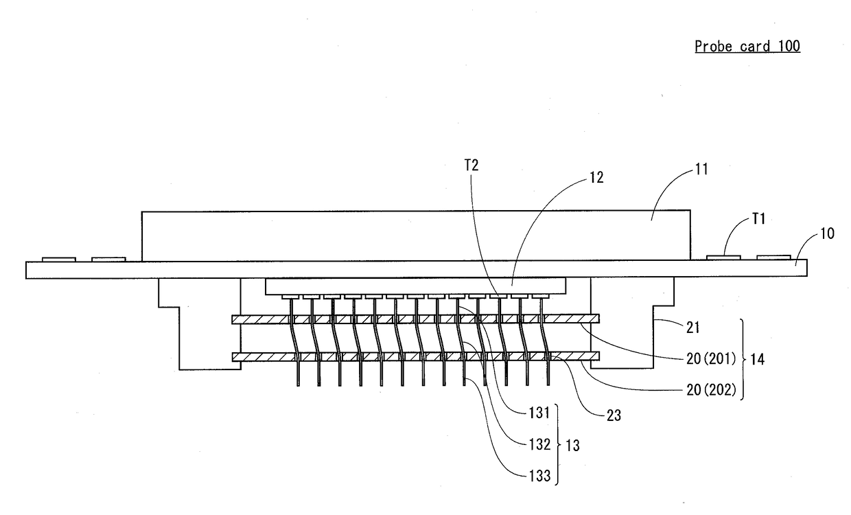
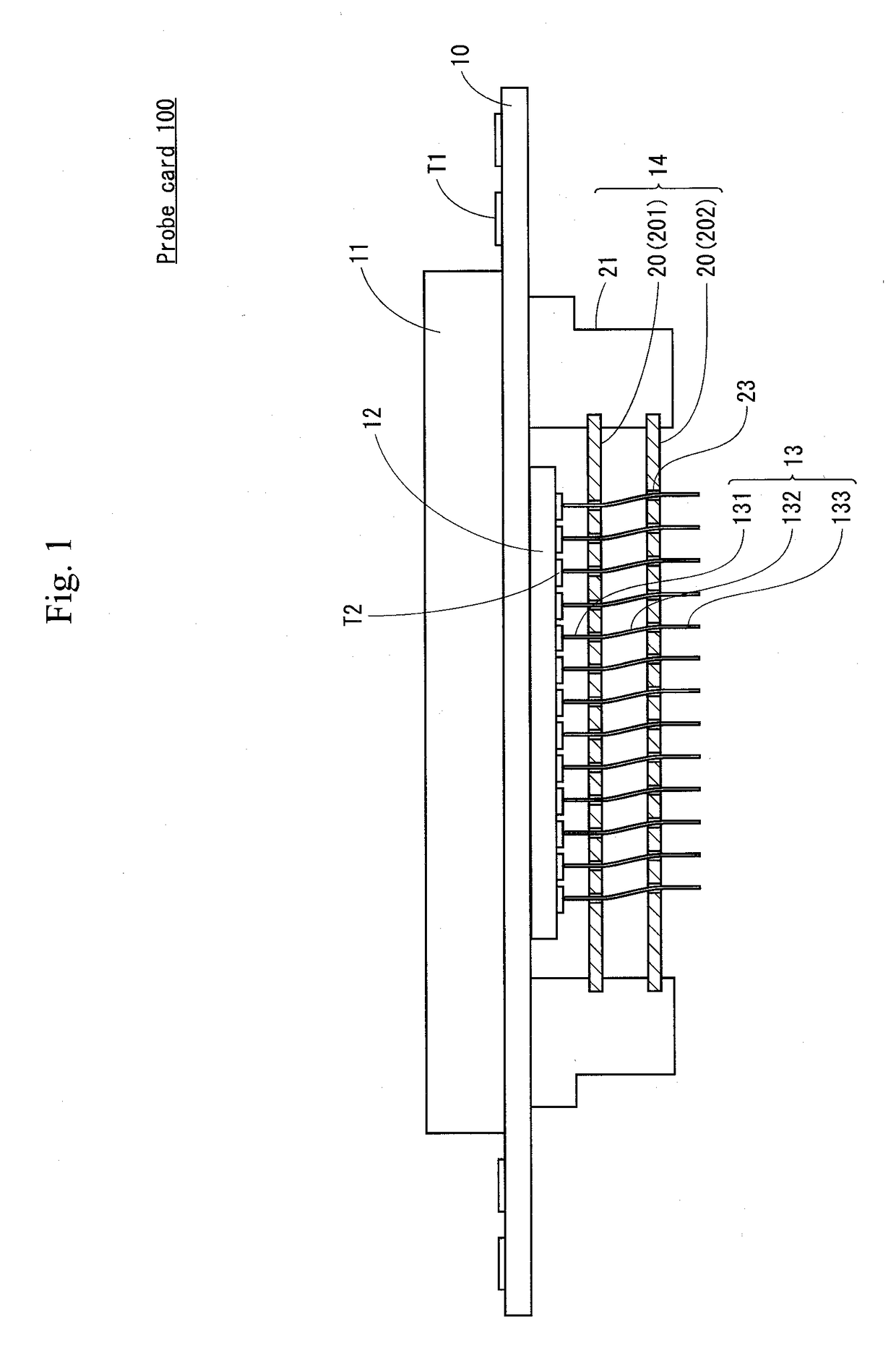
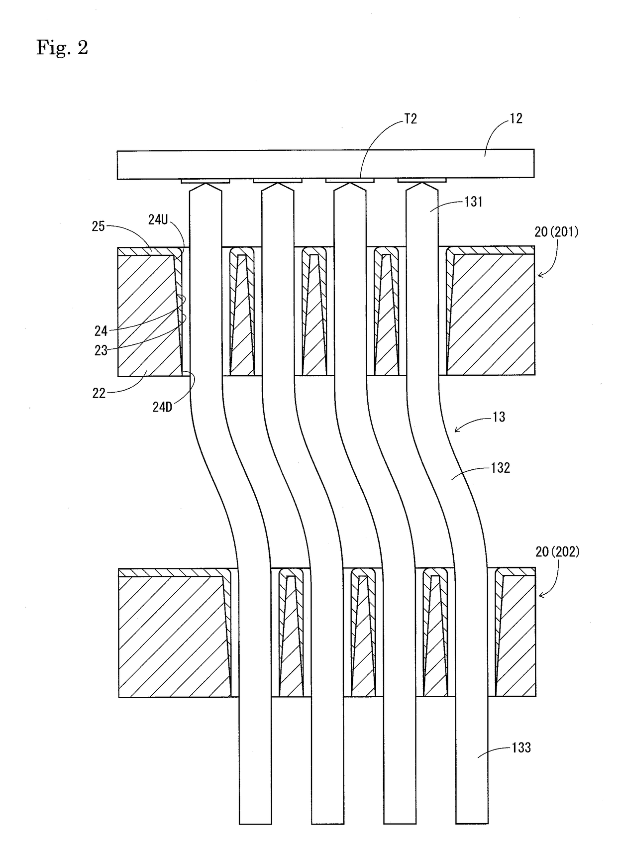
[0026]FIGS. 1 and 2 are diagrams illustrating a configuration example of a probe card 100 according to an embodiment of the present invention.

[0027]FIG. 1 illustrates a cross section when the probe card 100 arranged in the horizontal direction such that the contact probe 13 is on the lower side is cut along a vertical plane. FIG. 2 illustrates the detailed configuration of the contact probes 13 and the guide plates 20.

[0028]The probe card 100 is a device used in an inspection process of semiconductor integrated circuits, and configured to include a main board 10, a reinforcing plate 11, an ST (space transformer) board 12, the contact probes 13, and a probe guide 14.

[0029]The main board 10 is a wiring board adapted to be detachably attached to a prober (not illustrated), for example, a disk-shaped printed circuit board, and provided with a number of external electrodes T1. The external electrodes T1 are input / output terminals for inputting / outputting signals to / from a tester, and arr...


PUM


Abstract

OBJECT
To improve the strength of a probe guide and improve the abrasion resistance of the probe guide.
MEANS FOR SETTLEMENT
A guide plate 20 is formed of a silicon plate 22 having guide holes 23 respectively adapted to support contact probes 13, the inner walls of the guide holes 23 include a guide film 25 formed on the inner wall surfaces of corresponding penetration-processed holes 24 of the silicon plate 22, the cross-sectional areas of the penetration-processed holes 24 gradually increase toward a first surface of the silicon plate 22, and the film thickness of the guide film 25 gradually increases toward the first surface of the silicon plate 22. By employing such a configuration, as compared with the tilts of the inner wall surfaces of the penetration-processed holes 24, the tilts of the inner wall surfaces of the guide holes 23 can be suppressed, and the strength of the silicon plate 20 can be improved. Accordingly, the abrasion resistance of a probe guide 100 can be improved.

Description

TECHNICAL FIELD[0001]The present invention relates to a probe guide, a probe card, and a method for probe guide manufacturing, and more specifically, to improving a guide hole of a probe guide.BACKGROUND ART[0002]In general, a probe card is configured to provide a number of contact probes to stand on a wiring board, and used in an inspection process of semiconductor integrated circuits. A semiconductor integrated circuit is inspected by bringing contact probes into contact with corresponding electrode pads of the semiconductor integrated circuit formed on a semiconductor wafer and electrically connecting the semiconductor integrated circuit and an external device to each other. When doing this, in order to accommodate variations in the heights of contact probes and electrode pads and thereby surely electrically connect the contact probes and the electrode pads, a process to press the contact probes against the electrode pads is performed, correspondingly. This process is called over...

Claims


Application Information

Patent Timeline
Patent Type & Authority Applications(United States)
IPC IPC(8): G01R1/073G01R31/28G01R3/00
CPCG01R1/07371G01R1/07342G01R3/00G01R31/2886G01R1/07357G01R31/2863G01R31/2889
Inventor MORI, CHIKAOMISHIMIZU, YUICHIROFUJIHARA, KOSUKE
Owner SHINKO ELECTRIC IND CO LTD
Why Eureka
Try Eureka