Opto-electric hybrid board and method of manufacturing same

a hybrid board and opto-electric technology, applied in the field can solve the problems of increasing optical losses during optical coupling, difficult to ensure sufficient rigidity in the portion of opto-electric hybrid boards, and insufficient rigidity of proportions, so as to improve the rigidity of that portion, improve the rigidity, and increase the thickness of the metal reinforcement layer

Active Publication Date: 2017-10-05
NITTO DENKO CORP
View PDF6 Cites 1 Cited by
  • Summary
  • Abstract
  • Description
  • Claims
  • Application Information

AI Technical Summary

Benefits of technology

[0006]Unfortunately, while a portion of such an opto-electric hybrid board where interconnect lines extend is required to have a high degree of flexibility, an optical coupling portion with an optical element mounted thereon in the same opto-electric hybrid board and a portion of the same opto-electric hybrid board for connection to other members through a connector member attached thereto are required to be as rigid as possible from the viewpoint of handleability. Under the current circumstances, these portions tend to have insufficient rigidity. It is hence strongly desirable to increase the rigidity of these portions so as to prevent these portions from being influenced by warpage and thermal deformation during handling and during repeated use.

Problems solved by technology

Unfortunately, while a portion of such an opto-electric hybrid board where interconnect lines extend is required to have a high degree of flexibility, an optical coupling portion with an optical element mounted thereon in the same opto-electric hybrid board and a portion of the same opto-electric hybrid board for connection to other members through a connector member attached thereto are required to be as rigid as possible from the viewpoint of handleability.
Under the current circumstances, these portions tend to have insufficient rigidity.
This results in the increase in optical losses during the optical coupling, and is therefore not preferable.
For this reason, it is inevitably difficult to ensure sufficient rigidity in the portion of the opto-electric hybrid board which is used for connection to other members and the like.

Method used


Image

  • Opto-electric hybrid board and method of manufacturing same
  • Opto-electric hybrid board and method of manufacturing same
  • Opto-electric hybrid board and method of manufacturing same

Examples


Embodiment Construction

[0031]Next, an embodiment according to the present invention will now be described in detail with reference to the drawings. It should be noted that the present invention is not limited to this embodiment.

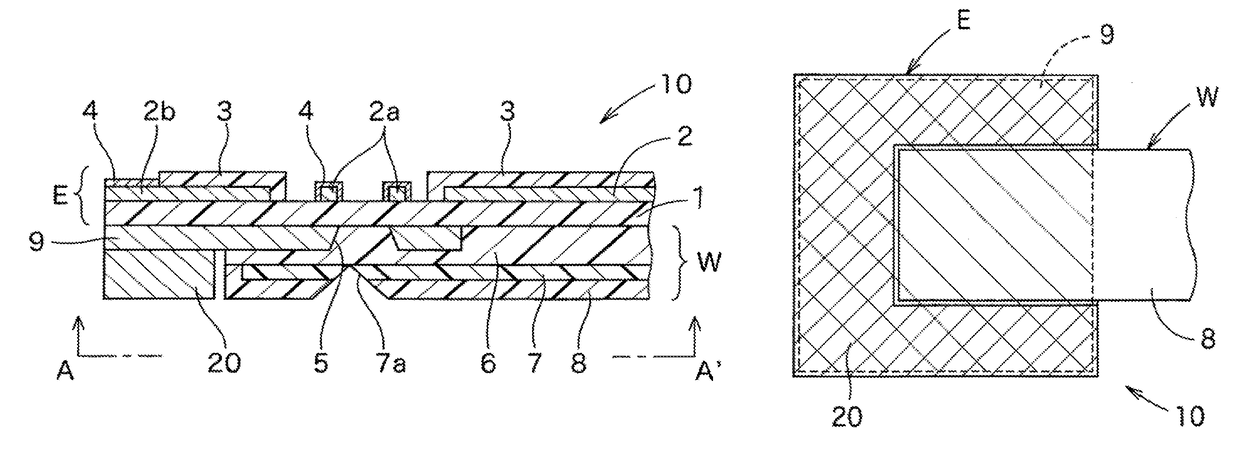
[0032]FIG. 1A is a schematic partial vertical sectional view of an opto-electric hybrid board according to one embodiment of the present invention, and FIG. 1B is a view as seen in the direction of the arrows A-A′ of FIG. 1A. This opto-electric hybrid board 10 includes: an electric circuit board E including an insulation layer 1 and electrical interconnect lines 2 provided on the front surface of the insulation layer 1; and an optical waveguide W provided on the back surface of the insulation layer 1.

[0033]In the electric circuit board E, the electrical interconnect lines 2 including optical element mounting pads 2a, a connector mounting pad 2b, other pads for mounting variable elements, grounding electrodes (not shown) and the like are formed on the front surface of the insulation...


PUM


Abstract

An opto-electric hybrid board includes: an electric circuit board including electrical interconnect lines formed on the front surface of an insulation layer; a metal reinforcement layer formed partially on the back surface of the electric circuit board; an optical waveguide W configured to partially overlap the back surface of the electric circuit board E; and an second reinforcement layer formed on the back surface of the electric circuit board E. The second reinforcement layer allows the opto-electric hybrid board to have improved rigidity in a specific region and excellent handleability without incurring optical losses during optical coupling.

Description

TECHNICAL FIELD[0001]The present invention relates to an opto-electric hybrid board including an electric circuit board and an optical wave guide which are stacked together, and a method of manufacturing the same.BACKGROUND ART[0002]With the increase in the amount of transmission information, optical interconnect lines in addition to electrical interconnect lines have been used in recent electronic devices and the like. A large number of opto-electric hybrid boards capable of transmitting electrical signals and optical signals at the same time have been used. As shown in FIG. 11, a known example of such opto-electric hybrid boards has a structure in which an electric circuit board E includes an insulation layer 1 made of polyimide and the like and serving as a substrate, and electrical interconnect lines 2 of an electrically conductive pattern provided on the front surface of the insulation layer 1, and in which an optical waveguide W is provided on the back surface of the insulatio...

Claims


Application Information

Patent Timeline
Patent Type & Authority Applications(United States)
IPC IPC(8): G02B6/43G02B6/42G02B6/12G02B6/136
CPCG02B6/43G02B6/12004G02B6/4214G02B6/136H05K1/02G02B6/4231G02B6/122G02B6/13H05K1/0274G02B6/4281
Inventor TSUJITA, YUICHITANAKA, NAOYUKI
Owner NITTO DENKO CORP
Why Eureka
Try Eureka