
Diode and power convertor using the same

a technology of diodes and power converters, applied in control systems, semiconductor devices, solid-state devices, etc., can solve problems such as adverse effects and breakdown of motor insulation, and achieve the effects of reducing carrier concentration, high resistance, and high resistan

Inactive Publication Date: 2017-11-02
HITACHI POWER SEMICON DEVICE
View PDF62 Cites 14 Cited by
  • Summary
  • Abstract
  • Description
  • Claims
  • Application Information

AI Technical Summary

Benefits of technology

The present invention provides a diode and a power convertor that can improve the performance of the diode by balancing its conduction loss and switching loss. It also prevents surge voltage and high frequency oscillation during reverse recovery switching while reducing leakage current that can cause damage to the diode. This invention maintains the dielectric strength of the diode.

Problems solved by technology

Accordingly, there arise concerns about adverse effects such as breakdown of motor insulation, element breakdown caused by overvoltage, and element malfunction.

Method used


Image

  • Diode and power convertor using the same
  • Diode and power convertor using the same
  • Diode and power convertor using the same

Examples


first embodiment

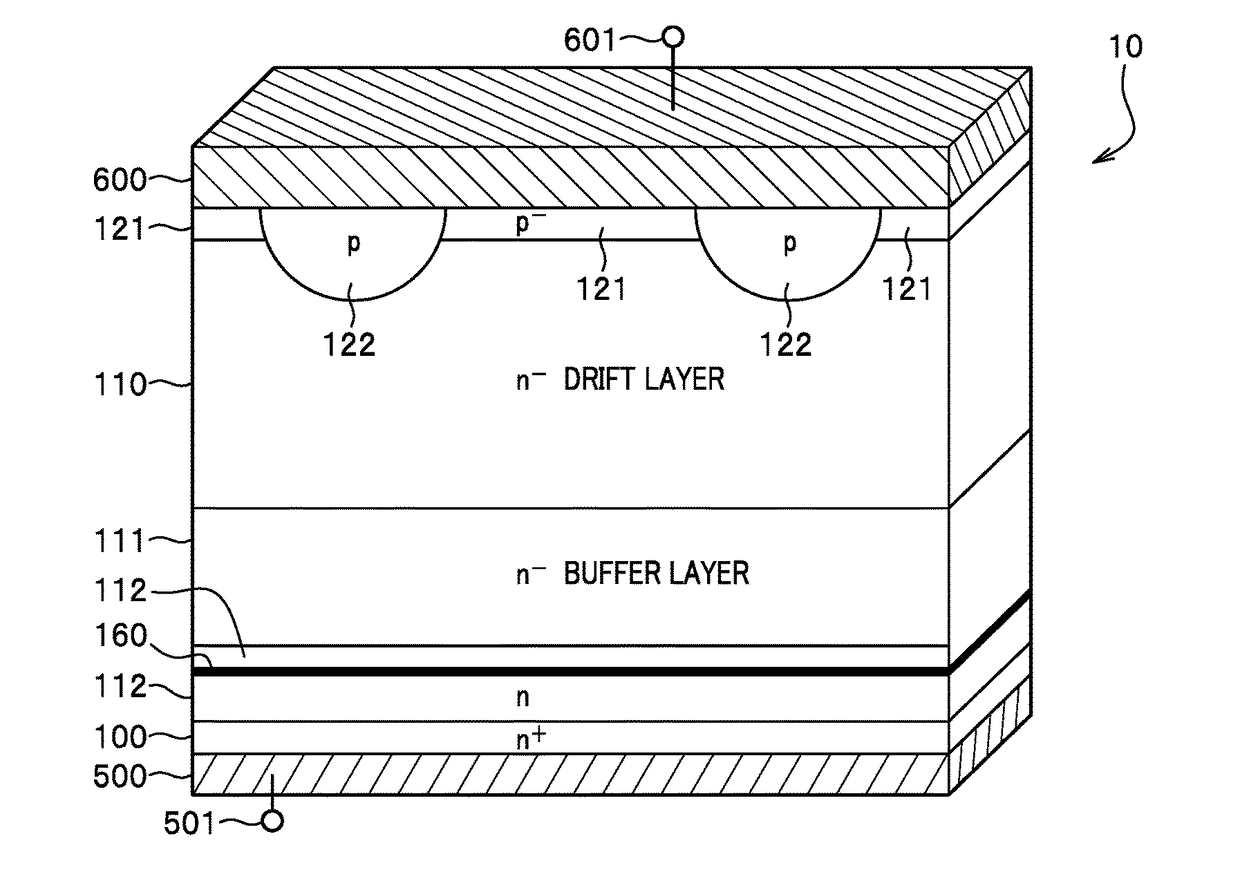
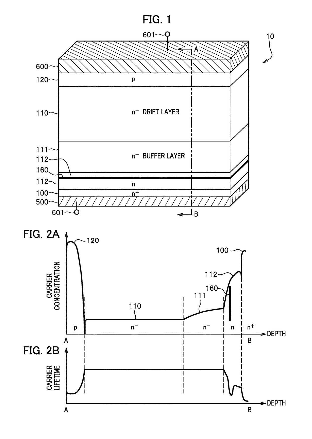
[0043]A diode 10 of a first embodiment of the present invention is described with reference to the drawings.

10>>

[0044]FIG. 1 is a diagram showing an example of an upper surface and a cross section of the diode 10 according to the first embodiment of the present invention.

[0045]In FIG. 1, the diode 10 is formed between an anode electrode layer 600 to which an anode electrode 601 is connected, and a cathode electrode layer 500 to which a cathode electrode 501 is connected.

[0046]Here, the anode electrode layer 600 and the cathode electrode layer 500 are layers mainly containing metal.

[0047]The anode electrode layer 600 is in contact with an upper surface (an upper surface in the drawing) of a p type semiconductor layer 120 (a second semiconductor layer of a second conductivity type).

[0048]A lower surface of the p type semiconductor layer 120 is in contact with an upper surface of an n− drift layer 110 (a first semiconductor layer of a first conductivity type).

[0049]A lower surface of t...

second embodiment

[0116]A diode 10 of a second embodiment of the present invention is described with reference to the drawings.

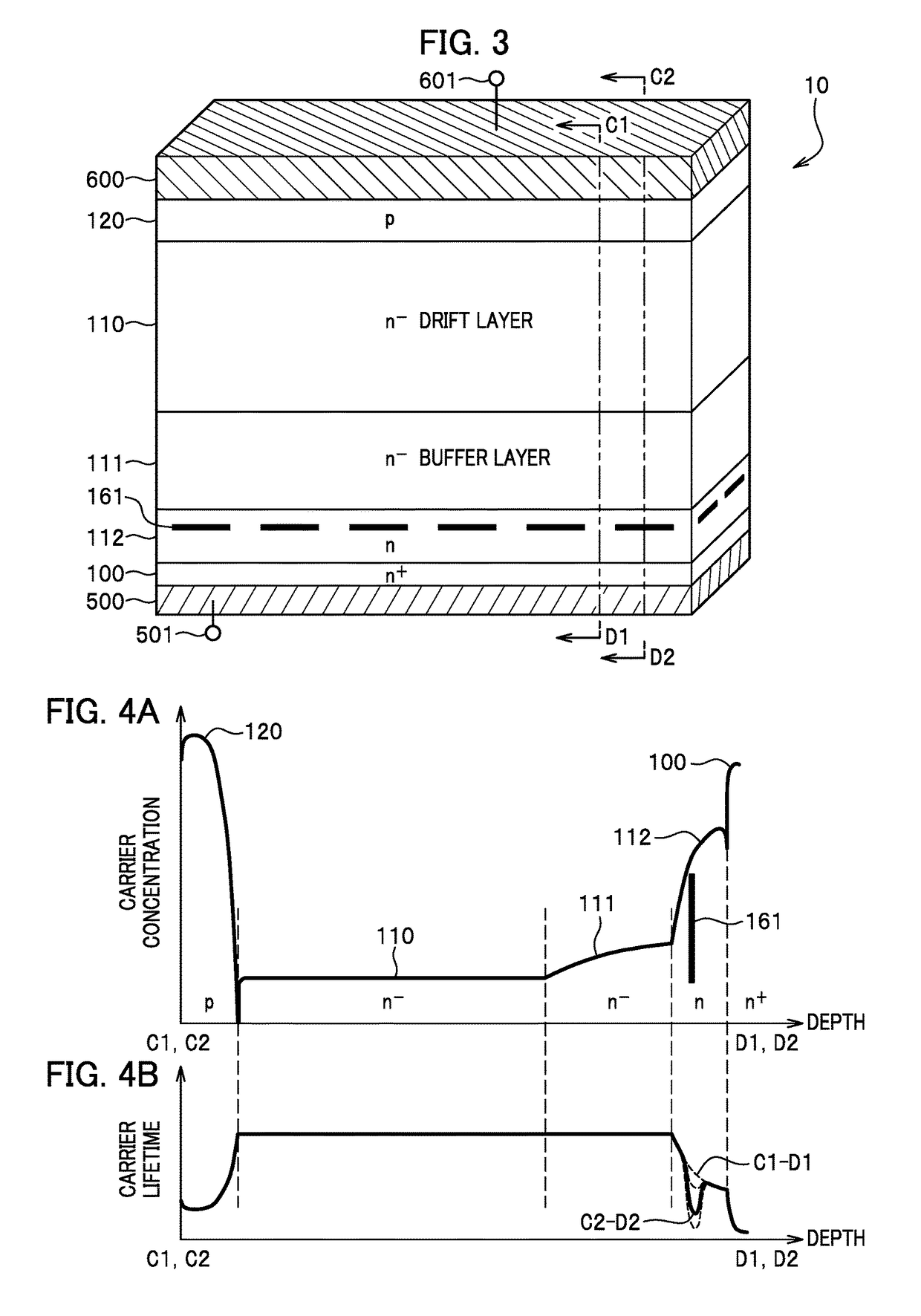
[0117]FIG. 3 is a diagram showing an example of an upper surface and a cross section of the diode 10 according to the second embodiment of the present invention.

[0118]In FIG. 3, what is different from FIG. 1 is a structure of a low carrier lifetime control layer 161.

[0119]The low carrier lifetime control layer 161 is formed partly inside a shallow n buffer layer 112. For example, the low carrier lifetime control layer 161 exists in a cross section taken along a line C2-D2 in FIG. 3 as in the low carrier lifetime control layer 160 in FIG. 1, but does not exist in a cross section taken alone a line C1-D1 in FIG. 3.

[0120]FIGS. 4A and 4B are diagrams showing an example of depth-direction cross-sectional profiles on cross sections, taken along the lines C1-D1 and C2-D2 in FIG. 3, of the diode 10 according to the second embodiment of the present invention. FIG. 4A presents a carrie...

third embodiment

[0127]A diode 10 of a third embodiment of the present invention is described with reference to the drawings.

[0128]FIG. 5 is a diagram showing an example of an upper surface and a cross section of the diode 10 according to the third embodiment of the present invention.

[0129]In FIG. 5, what is different from FIG. 1 is that a low carrier lifetime control layer 162 is provided in a deep n− buffer layer 111. More specifically, the shallow n buffer layer 112 in FIG. 1 is not present but the deep n− buffer layer 111 also serves as the shallow n buffer layer 112 of the n type.

[0130]Here, the high-concentration n+ layer 100 in FIG. 1 is presented as a high-concentration n+ layer 104 in FIG. 5.

[0131]Moreover, FIG. 5 showing the third embodiment is different from FIG. 1 showing the first embodiment only in the absence of the shallow n buffer layer 112, and the positional relationship between the deep n− buffer layer 111 and the low carrier lifetime control layer 161. For this reason, the redun...


PUM


Abstract

A diode includes an anode electrode layer; a cathode electrode layer; a buffer layer of a first conductivity type formed between the anode electrode layer and the cathode electrode layer in a region extending to a location at a distance of 30 μm or more from the cathode electrode layer; a first semiconductor layer of the first conductivity type formed in a region between the anode electrode layer and the cathode electrode layer, and being in contact with the buffer layer of the first conductivity type; and a second semiconductor layer of a second conductivity type formed in a region between the anode electrode layer and the first semiconductor layer of the first conductivity type. The carrier concentration in the first semiconductor layer is lower than the carrier concentration in the buffer layer. The carrier concentration in the buffer layer is less than 1×1015 cm−3.

Description

BACKGROUND OF THE INVENTION1. Field of the Invention[0001]The present invention relates to a diode and a power convertor using the same.2. Background Art[0002]A power convertor uses diodes as freewheel diodes connected in anti-parallel to insulated gate bipolar transistors (IGBTs) or metal oxide semiconductor field effect transistors (MOS transistors). Such diodes have been required to reduce losses from the viewpoint of energy saving and to reduce noise for reliability and controllability.[0003]As typical losses of the diode, there are a forward voltage drop (VF: Forward Voltage) equivalent to a turn-on loss, and a reverse recovery switching loss (Err: Reverse Recovery Loss). Main contributors to reductions in the losses of power conversion systems are a reduction in VF in the case of low drive frequency devices such as convertors, and a reduction in Err in the case of high drive frequency devices such as inverters. Hence, in recent years, there has been a demand for further reduct...

Claims


Application Information

Patent Timeline
Patent Type & Authority Applications(United States)
IPC IPC(8): H01L27/08H02M7/537H02M1/084H01L29/861H01L29/417H02P27/06H01L29/36
CPCH01L27/0814H01L29/41716H01L29/36H02P27/06H02M7/537H02M1/084H01L29/861H01L27/0255H01L29/32H01L29/66136
Inventor ARAI, TAIGAWAKAGI, MASATOSHIISHIMARU, TETSUYAMORI, MUTSUHIRO
Owner HITACHI POWER SEMICON DEVICE
Learn More