Laser dicing device

a laser dicing and dicing technology, applied in the direction of manufacturing tools, instruments, welding/soldering/cutting articles, etc., can solve the problems of inability to quickly and accurately detect and the autofocus mechanism does not function normally, so as to achieve accurate and stably the height position of the wafer surface.

Active Publication Date: 2017-11-09
TOKYO SEIMITSU
View PDF1 Cites 10 Cited by
  • Summary
  • Abstract
  • Description
  • Claims
  • Application Information

AI Technical Summary

Benefits of technology

[0013]The present invention has been made in view of such circumstances and aims to provide a laser dicing device which can perform detection of the height position of the laser beam irradiation surface of the wafer accurately and stably without being affected by the variation in the thin film formed on the laser beam irradiation surface of the wafer.
[0023]According to the present invention, the height position of a surface of the wafer can be detected accurately and stably without being affected by variation in a thin film formed on the laser beam irradiation surface of the wafer. As a result, the modified regions can be formed with accuracy at a predetermined processing depth from the surface of the wafer.

Problems solved by technology

Thus, a reflectance of the detection laser beam may be lowered by the variation by each wafer or the variation by each place on the rear surface of one wafer, which leads to a problem that the autofocus mechanism does not function normally due to the variations.
That is, the variation by each wafer and the variation by each place of a thin film formed on the rear surface of one wafer give an influence on an operation of the autofocus mechanism, which leads to a problem that detection of the height position of the wafer surface cannot be performed rapidly and stably with accuracy.
Here, similar problem may occur not only when the rear surface of the wafer W is irradiated with the laser beam, but also when the front surface (device surface) of the wafer W is irradiated with the laser beam irradiation.

Method used


Image

  • Laser dicing device
  • Laser dicing device
  • Laser dicing device

Examples


first embodiment

[0068]First, a first embodiment of the present invention is described.

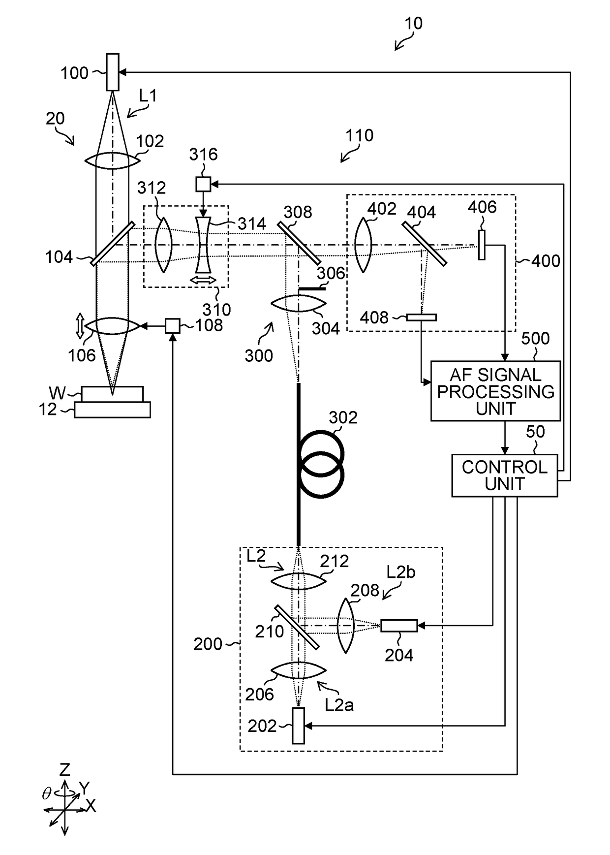
[0069]FIG. 1 is a block diagram illustrating an outline of a laser dicing device according to a first embodiment. As illustrated in FIG. 1, the laser dicing device 10 includes a stage 12, a laser head 20, a control unit 50 and the like.

[0070]The stage 12 is configured to be movable in XYZθ directions and suctions and holds a wafer W. The wafer W is placed on the stage 12 so that a rear surface on a side opposite to a front surface (device surface) becomes a surface (laser beam irradiation surface) to be irradiated with a laser beam. Here, the front surface of the wafer W may be the laser beam irradiation surface. The same applies to the other embodiments which will be described later.

[0071]The laser head 20 irradiates the wafer W with a processing laser beam L1 for forming a modified region inside the wafer W.

[0072]The control unit 50 includes a CPU (Central Processing Unit), a memory, an input / output circuit port...

second embodiment

[0164]Subsequently, a second embodiment of the present invention is described. Hereinafter, description is omitted for portions in common with the first embodiment, and mainly feature portions of this embodiment are described.

[0165]FIG. 17 is a block diagram illustrating an outline of a laser dicing device according to the second embodiment. In FIG. 17, constituent elements in common or similar to those in FIG. 1 are given the same reference numerals, and description thereof is omitted.

[0166]The second embodiment uses an astigmatism method as a method for detecting a height position of a laser beam irradiation surface of a wafer W.

[0167]As illustrated in FIG. 17, the AF laser beam L2 output from the light source unit 200 of the AF device 110 goes through the optical fiber 302, is collimated by the collimate lens 304 and is reflected by the half mirror 308 without having a part of the AF laser beam L2 shielded. Moreover, this AF laser beam L2 is converged by the light converging lens...

third embodiment

[0179]Subsequently, a third embodiment of the present invention is described. Hereinafter, description is omitted for portions in common with the first embodiment, and mainly feature portions of this embodiment are described.

[0180]FIG. 20 is a block diagram illustrating an outline of a laser dicing device according to the third embodiment. In FIG. 20, constituent elements in common or similar to those in FIG. 1 are given the same reference numerals, and description thereof is omitted.

[0181]The third embodiment uses a central intensity method as a method for detecting the height position of the laser beam irradiation surface of the wafer W. The central intensity method is a method in which a part of the reflection light is received by either one of the two detectors, while the whole of or a part of the reflection light is received by the other detector, and the height position of the laser beam irradiation surface of the wafer W is detected by using the light receiving amounts in the...


PUM

PropertyMeasurementUnit
thicknessaaaaaaaaaa
wavelengthaaaaaaaaaa

Abstract

A height position of a surface of a wafer can be detected accurately and stably without being affected by variation in a thin film formed on the surface of the wafer. An AF (autofocus) device irradiates the surface of the wafer W with an AF laser beam, detects reflection light thereof for each wavelength with a detection optical system. An AF signal processing unit outputs a displacement signal indicating displacement of the surface of the wafer to a control unit on the basis of a detection result of the detection optical system. Moreover, the AF device includes a focus optical system disposed in an irradiation optical path which is an optical path from the light source unit to a light converging lens. The focus optical system adjusts a light converging point of the AF laser beam in a wafer thickness direction.

Description

CROSS-REFERENCE TO RELATED APPLICATIONS[0001]This application is a Continuation of PCT International Application No. PCT / JP2016 / 052003 filed on Jan. 25, 2016, which claims priority under 35 U.S.C. §119(a) to Japanese Patent Application Nos. 2015-014325 and 2015-014327 filed on Jan. 28, 2015. Each of the above application(s) is hereby expressly incorporated by reference, in its entirety, into the present application.BACKGROUND OF THE INVENTIONField of the Invention[0002]The present invention relates to a laser dicing device which divides a wafer on which semiconductor devices, electronic components and the like are formed into individual chips.Description of the Related Art[0003]Conventionally, when a wafer on whose surface semiconductor devices, electronic components and the like are formed is divided into individual chips, a dicing device has been used. The dicing device forms grinding grooves in the wafer with a thin grinding stone having a thickness of approximately 30 μm and for...

Claims


Application Information

Patent Timeline
Patent Type & Authority Applications(United States)
IPC IPC(8): B23K26/046B23K26/00H01L21/67G01B11/06B23K26/53B23K26/03B23K26/06B23K101/40B23K103/00H01L21/78
CPCB23K26/046B23K26/0006B23K26/0057B23K26/53B23K26/032H01L21/78G01B11/0608H01L21/67092H01L21/67259B23K2201/40B23K2203/56B23K26/0648B23K26/0622B23K2101/40B23K2103/56G01B11/00
Inventor HYAKUMURA, KAZUSHI
Owner TOKYO SEIMITSU
Why Eureka
Try Eureka