Signal processing device, imaging element, and electronic apparatus
a technology of imaging element and signal processing device, which is applied in the field of signal processing device, imaging element, electronic apparatus, etc., can solve the problems of circuit area increase and cost increase, and achieve the effect of suppressing the cost increas
- Summary
- Abstract
- Description
- Claims
- Application Information
AI Technical Summary
Benefits of technology
Problems solved by technology
Method used
Image

Examples
first embodiment
1. First Embodiment
[0062]
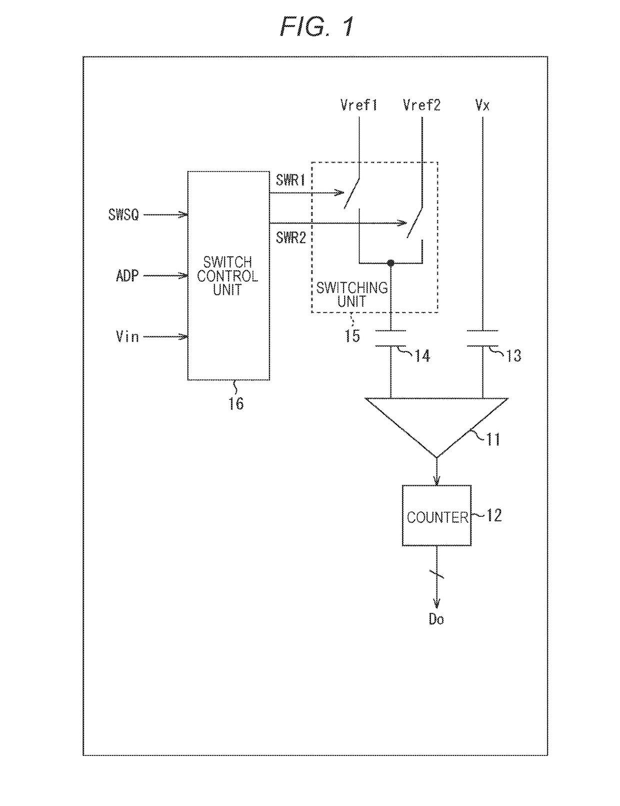
[0063]Typically, a general image sensor has been configured to read, as a signal, electrical charge stored in a light receiving unit such as a photodiode to perform analog / digital (A / D) conversion of the electrical charge. Such A / D conversion has been generally performed in such a manner that a signal read from a pixel having the light receiving unit is compared with a reference voltage such as a ramp wave and a time until such a comparison result changes is measured.
[0064]Gradation enhancement of the image sensor is one type of performance required for image quality enhancement. In particular, gradation enhancement in a low-illuminance region greatly contributes to an image quality. Generally, in the case of enhancing a gradation, such enhancement sacrifices high-speed performance, an area, and power consumption. Due to gradation enhancement, the number of A / D conversion processes increases, and this might lead to lowering of the high-speed performance. Fur...
second embodiment
2. Second Embodiment
[0144]
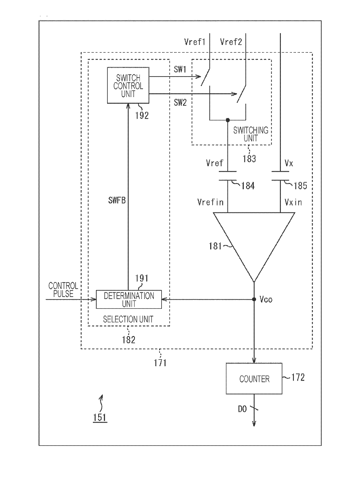
[0145]In the first embodiment, reduction in the error due to the change in the coupling voltage fluctuation amount in comparison of the reset signal and comparison of the pixel signal has been described. Similarly, upon completion of initialization of the comparison unit 11 and completion of determination of the signal level of the pixel signal, when the fluctuation amount of the coupling voltage on the floating node of the comparison unit 11 changes, this might lead to a determination error.
[0146]
[0147]For the above-described reasons, a signal line which is included in a selection unit configured to select, from a plurality of reference signals, a reference signal to be supplied to an input terminal as a floating node of a comparison unit and in which a parasitic capacitance is caused between the signal line and the input node as the floating node of the comparison unit is configured to transmit the same level of signal in both of initialization of the com...
third embodiment
3. Third Embodiment
[0156]
[0157]In each of the above-described embodiments, the signal line between the comparison unit 171 (the comparison unit 181) and the counter 172 is illustrated as connection via a single line for the sake of description. In fact, a plurality of signal lines connect between the comparison unit 171 (the comparison unit 181) and the counter 172 as in an example of FIG. 15, for example.
[0158]In the example of FIG. 15, each column A / D conversion unit 151 includes a latch 301 and a latch 302. The latch 301 is illustrated as a simple form of a selection unit 182 (FIG. 9). The output Vco of the comparison unit 181 in a period for determining the signal level of a pixel signal is latched by the latch 301, and control signals (a control signal SW1 and a control signal SW2) corresponding to such a value are supplied to a switching unit 183.
[0159]Moreover, on the basis of the latched output Vco of the comparison unit 181, the latch 301 supplies the latch 302 with an iden...
PUM
 Abstract
Description
Claims
Application Information
 - R&D
- Intellectual Property
- Life Sciences
- Materials
- Tech Scout
- Unparalleled Data Quality
- Higher Quality Content
- 60% Fewer Hallucinations
Browse by: Latest US Patents, China's latest patents, Technical Efficacy Thesaurus, Application Domain, Technology Topic, Popular Technical Reports.
© 2025 PatSnap. All rights reserved.Legal|Privacy policy|Modern Slavery Act Transparency Statement|Sitemap|About US| Contact US: help@patsnap.com