
Light emitting device and method of fabricating the same

a technology of light emitting devices and light leakage regions, which is applied in the direction of semiconductor devices, basic electric elements, electrical equipment, etc., can solve the problems of reducing the substantial light extraction energy from the light leakage region, increasing the electrode area, and increasing the amount of light extraction energy, so as to increase the flux extractable, increase the current spreading effect, and make the current spreading effect more distinctiv

Active Publication Date: 2009-03-31
SHIN-ETSU HANDOTAI CO LTD
View PDF11 Cites 6 Cited by
  • Summary
  • Abstract
  • Description
  • Claims
  • Application Information

AI Technical Summary

Benefits of technology

[0011]In the light emitting device of this invention, the thickness of the transparent thick-film semiconductor layer is limited to 10 μm or more, because it is intended to increase the luminance (integrating sphere luminance) of the entire light emitting device, by increasing the flux extractable from the side faces of the transparent thick-film semiconductor layer when the emission flux is extracted from the light emitting layer portion through that layer. The transparent thick-film semiconductor layer is composed of a III-V compound semiconductor having a band gap energy larger than a light quantum energy which corresponds to a peak wavelength of emission flux from the light emitting layer portion, because it is intended to suppress light absorption by such transparent thick-film semiconductor layer, and to increase the light extraction efficiency. The thickness of the transparent thick-film semiconductor layer is preferably 40 μm or more.
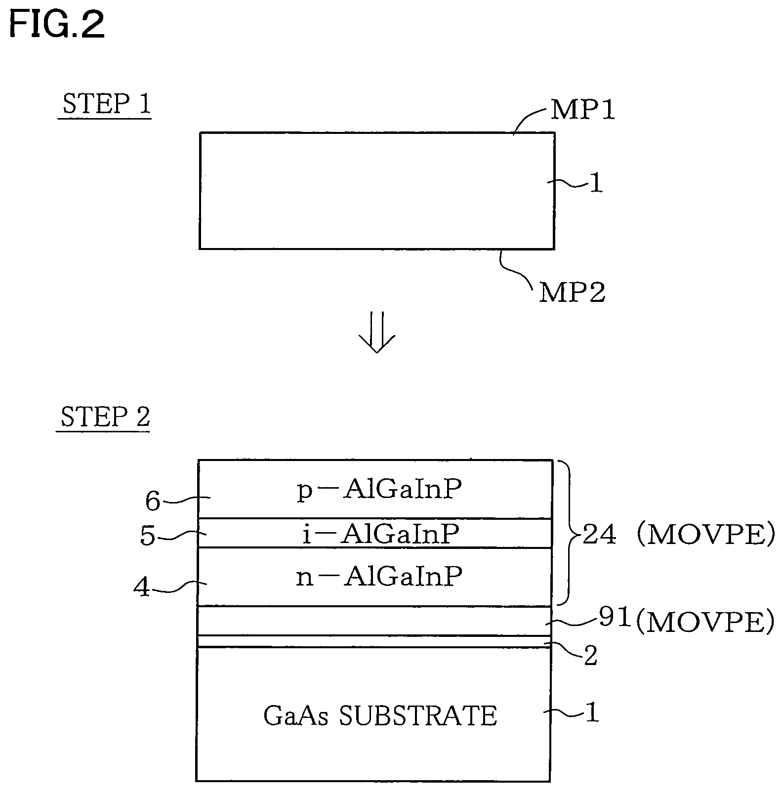
[0024]On the other hand, the transparent thick-film semiconductor layer can also be configured as being epitaxially grown on the light emitting layer portion by the hydride vapor phase epitaxial growth method (also referred to as the HVPE method, hereinafter). The HVPE method is a method such as converting Ga (gallium), having a low vaporizing pressure, into more vaporizable GaCl through reaction with hydrogen chloride, and allowing Ga to react with a Group V element source gas through the GaCl as a medium, so as to epitaxially grow a III-V compound semiconductor layer. For example, the light emitting layer portion composed of AlGaInP is generally formed by the metal organic vapor phase epitaxy method (also referred to as the MOVPE method, hereinafter), showing a layer growth rate of only as small as approximately 4 μm / hour or around, which could be appropriate for growth of a thin light emitting layer portion, but apparently disadvantageous for growth of a thick light emitting layer portion having a thickness of over 40 μm in terms of the process efficiency. In contrast to this, the growth rate of layers in the HVPE method is, for example approximately 9 μm / hour, which is more than twice larger than that in the MOVPE method, proving that the HVPE method can obtain a growth rate of layer larger than in the MOVPE method, so that the transparent thick-film semiconductor layer can be formed in an extremely efficient manner, and cost for the source materials can be suppressed to a far lower level than in the MOVPE method because there is no need of using any expensive organic metals.

Problems solved by technology

Conventional efforts have been made on increase in the energy of light extraction by effectively spreading current within the device through consideration on planary shape of the electrode, but increase in the electrode area is inevitable anyhow in this case, having been fallen in a dilemma that a smaller light extraction area results in a limited amount of energy of light extraction.
Another problem resides in that the current is less likely to spread in the in-plane direction, because the dopant carrier concentration, and consequently the conductivity, of the cladding layer is suppressed to a slightly lower level in order to optimize emissive recombination of carriers in the active layer.
This concentrates the current into the region covered by the electrode, and results in decreasing an amount of the substantial light extraction energy from the light leakage region.
The removal of the process-damaged layer by any publicly-known chemical etching, however, cannot always be judged by leakage current, because the light emitting layer portion and the transparent thick-film semiconductor layer differ in the chemical composition from each other, and this has been consequently resulting in only an insufficient improvement in the light extraction efficiency from the side face portions of these layers.
A method relying upon an excessively strong chemical etching, in view of raising the etching effect of the side face portions, is not adoptable because it may result in roughening of the main surface of the device or in damage of the metal electrodes already formed thereon, and may degrade performances of the device.

Method used


Image

  • Light emitting device and method of fabricating the same
  • Light emitting device and method of fabricating the same
  • Light emitting device and method of fabricating the same

Examples


Embodiment Construction

[0034]Best modes for carrying out this invention will be described below referring to the attached drawings.

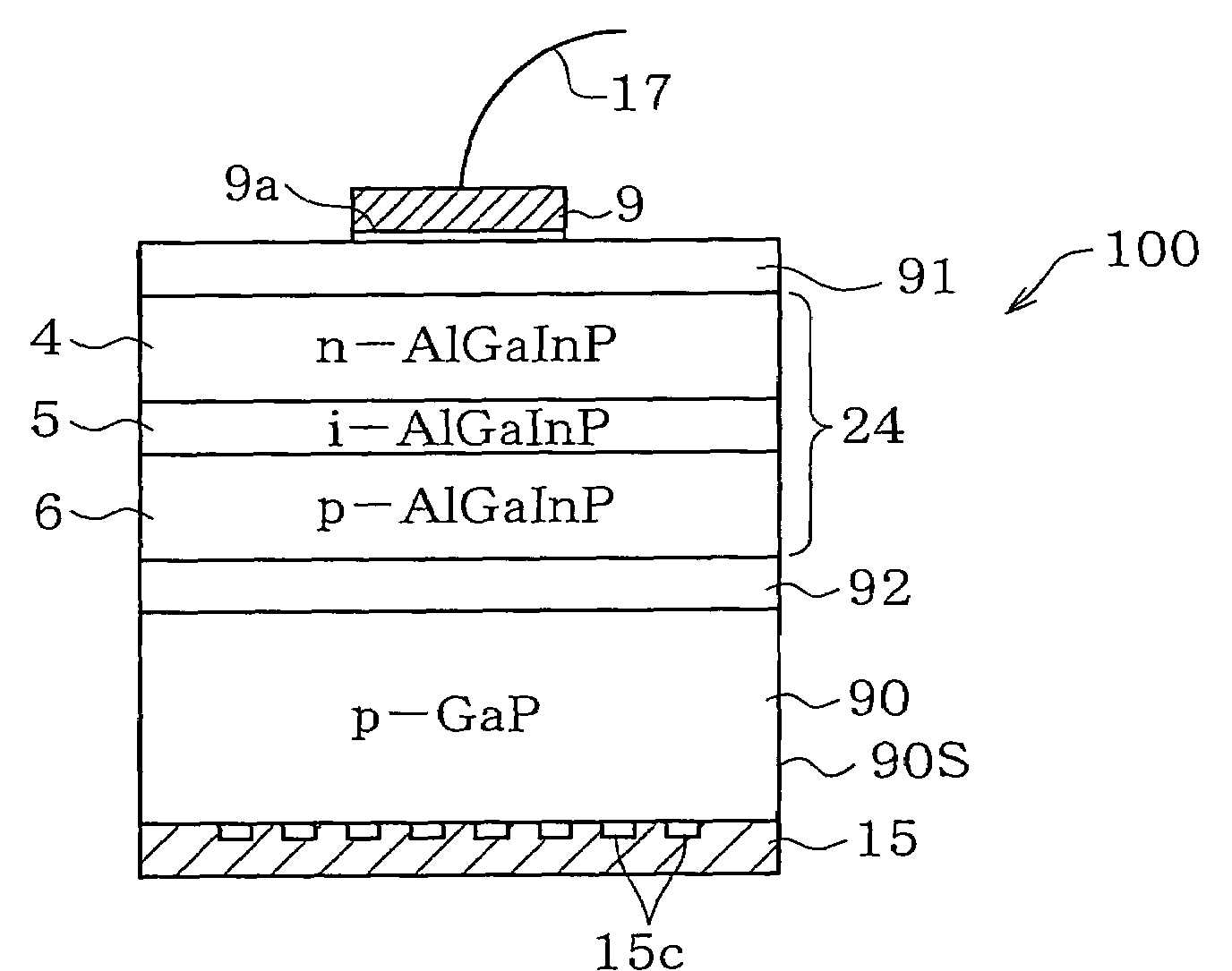
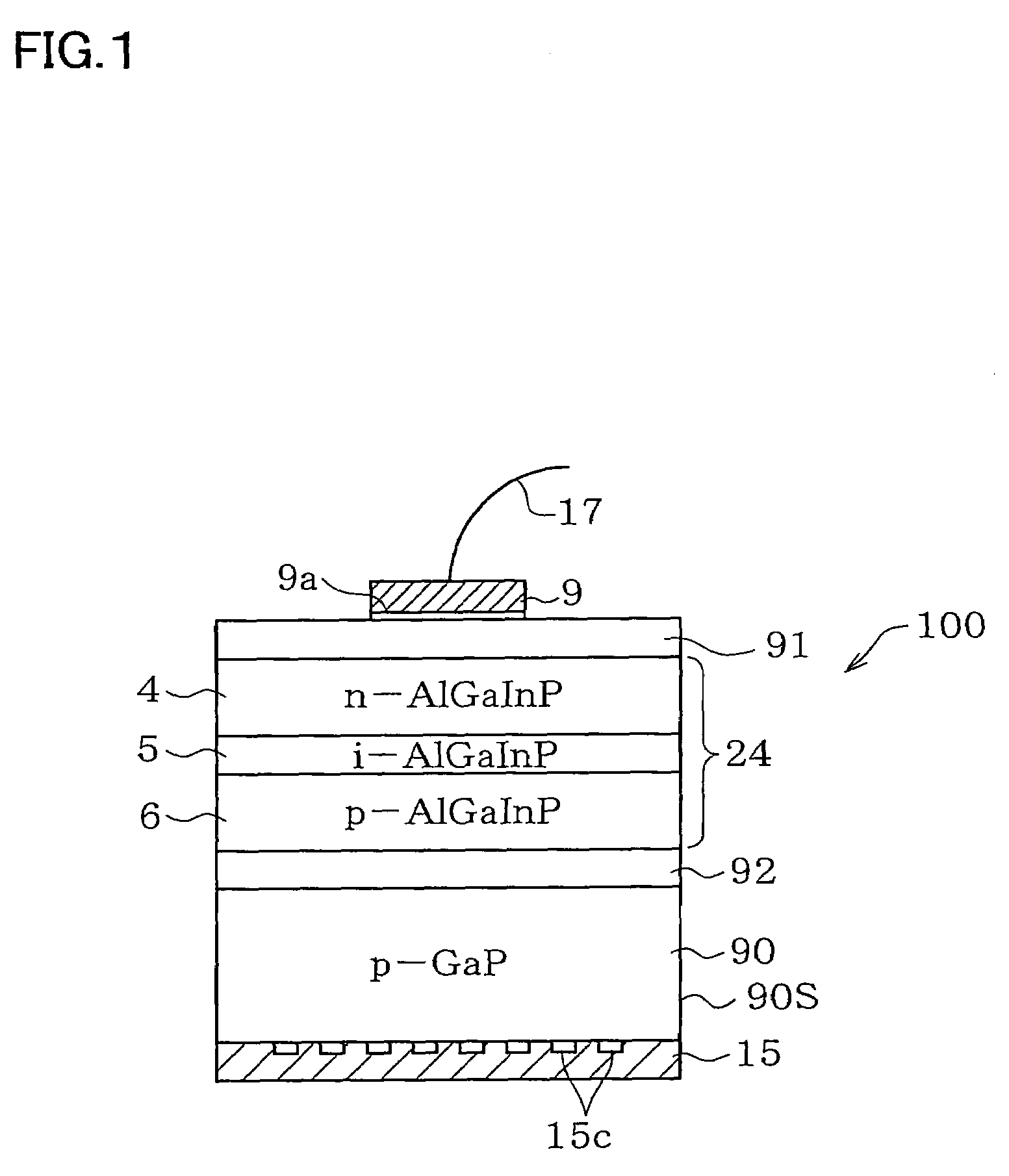
[0035]FIG. 1 is a conceptual drawing of a light emitting device 100 as one embodiment of this invention. The light emitting device 100 has a light emitting layer portion 24 composed of a III-V compound semiconductor; and a transparent thick-film semiconductor layer 90 formed on the second main surface side of the light emitting layer portion 24, and composed of a III-V compound semiconductor having a band gap energy larger than a light quantum energy which corresponds to a peak wavelength of emission flux from the light emitting layer portion 24.

[0036]The light emitting layer portion 24 has a structure in which an active layer 5 composed of a non-doped (AlxGa1−x)yIn1−yP alloy (where, 0≦x≦0.55, 0.45≦y≦0.55) is held between a p-type cladding layer 6 composed of a p-type (AlzGa1−z)yIn1−yP alloy (where, x4 composed of an n-type (AlzGa1−z)yIn1−yP alloy (where, x100 shown in FIG. 1,...


PUM


Abstract

Disclosed is a light-emitting device (100) has a light-emitting layer portion (24) which is composed of a group III-V compound semiconductor and a transparent thick-film semiconductor layer (90) with a thickness of not less than 40 μm which is formed on at least one major surface side of the light-emitting layer portion (24) and composed of a group III-V compound semiconductor having a band gap energy larger than the photon energy equivalent of the peak wavelength of emission flux from the light-emitting layer portion (24). The transparent thick-film semiconductor layer (90) has a lateral surface portion (90S) which is a chemically etched surface. The dopant concentration of the transparent thick-film semiconductor layer (90) is not less than 5×10¹⁶ / cm3 and not more than 2×10¹⁸ / cm3. The light-emitting device can have a transparent thick-film semiconductor layer while being significantly improved in light taking-out efficiency from the lateral surface portion.

Description

BACKGROUND OF THE INVENTION[0001]1. Field of the Invention[0002]This invention relates to a light emitting device and a method of fabricating the same.[0003]2. Description of the Related Art[0004]Light emitting device having the light emitting layer portion thereof composed of an (AlxGa1−x)yIn1−yP alloy (where, 0≦x≦1, 0≦y≦1; simply referred to as AlGaInP alloy, or more simply as AlGaInP, hereinafter) can be realized as a high-luminance device, by adopting a double heterostructure in which a thin AlGaInP active layer is sandwiched between an n-type AlGaInP cladding layer and a p-type AlGaInP cladding layer, both having a larger band gap. Current is supplied to the light emitting layer portion through a metal electrode formed on the surface of the device. The metal electrode acts as a light interceptor, so that it is formed, for example, so as to cover only the center portion of a first main surface of the light emitting layer portion, to thereby allow light to be extracted from the p...

Claims


Application Information

Patent Timeline
Patent Type & Authority Patents(United States)
IPC IPC(8): H01L29/26H01L21/205H01L33/00H01L33/14H01L33/30H01L33/40
CPCH01L33/30H01L21/02392H01L21/02395H01L21/02461H01L21/02505H01L21/02543H01L21/02579H01L21/0262H01L33/0079H01L33/14H01L33/405Y10S438/936H01L33/0093
Inventor YAMADA, MASATOSHINOHARA, MASAYUKITAKAHASHI, MASANOBUADOMI, KEIZOUIKEDA, JUN
Owner SHIN-ETSU HANDOTAI CO LTD
Learn More