
High current potted inductor and a method of manufacturing same

Inactive Publication Date: 2017-11-23
WARNER POWER ACQUISITION LLC
View PDF0 Cites 9 Cited by
  • Summary
  • Abstract
  • Description
  • Claims
  • Application Information

AI Technical Summary

Benefits of technology

The present invention relates to a high current potted inductor and a method of manufacturing the same that can handle both low and high frequency components of current. The technical effects of the invention include the ability to manage a low frequency component such as DC, as well as AC and high frequency components in the conductor. The invention also includes a thermal management structure to efficiently remove heat from the device and reducing the surface temperature of the structure. The invention solves the problem of high current devices being unable to handle high frequency components due to the substantially increased conductor and core losses.

Problems solved by technology

These devices in general are not well suited to handle higher frequencies due to the substantially increased conductor and core losses.
Higher frequency materials are also very limited due to their low saturation flux, therefore a solution to these products will be complex and very expensive.

Method used


Image

  • High current potted inductor and a method of manufacturing same
  • High current potted inductor and a method of manufacturing same
  • High current potted inductor and a method of manufacturing same

Examples


first embodiment

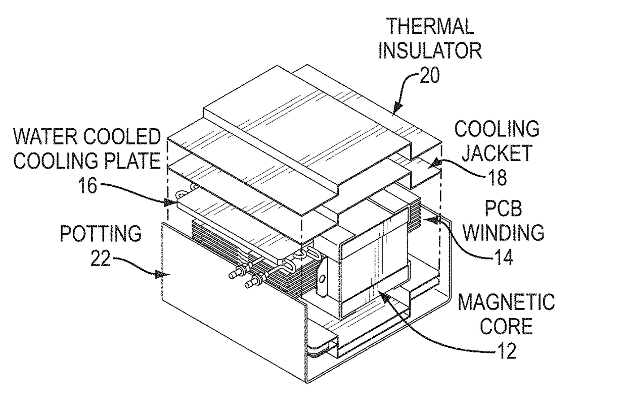
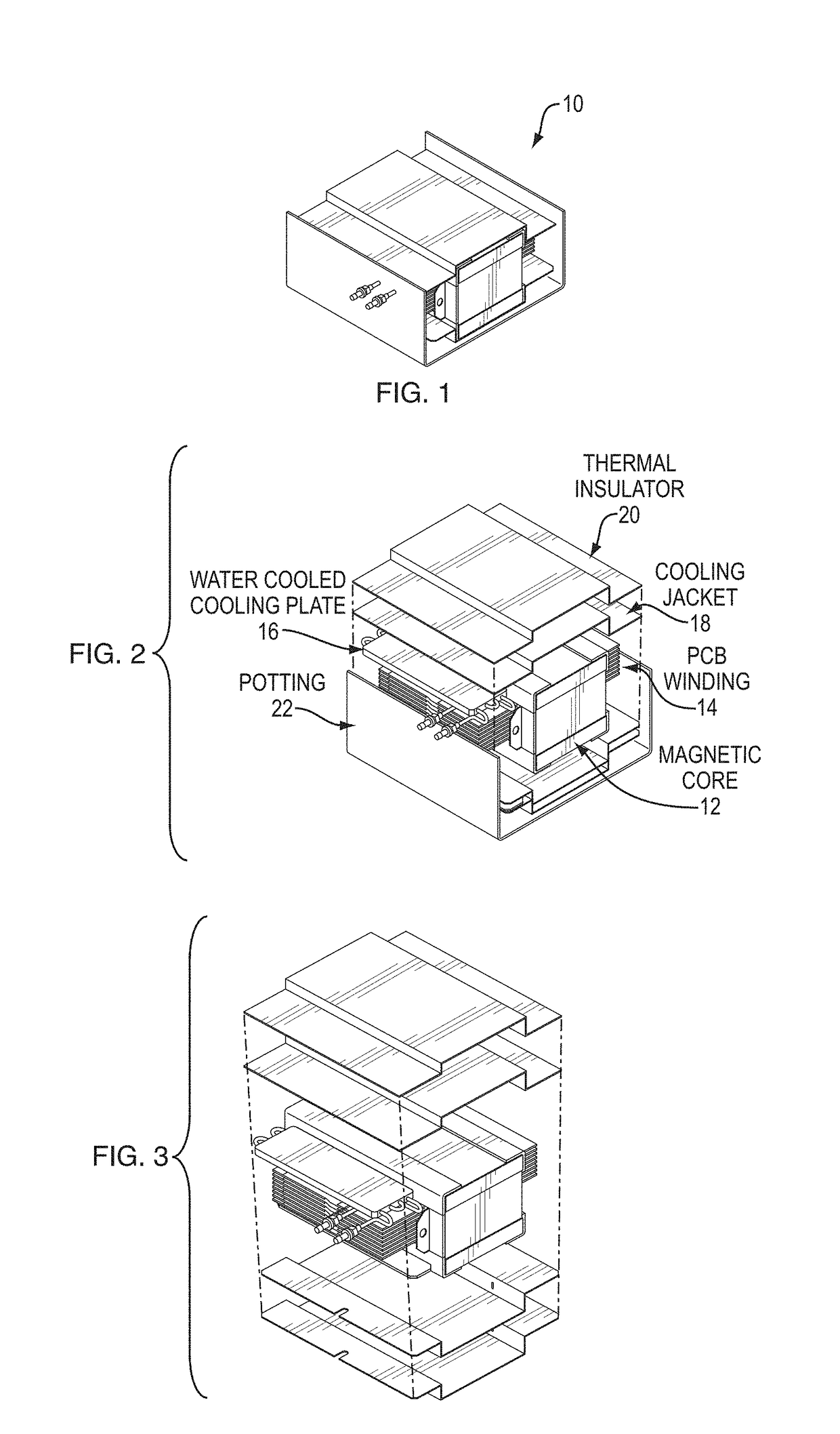
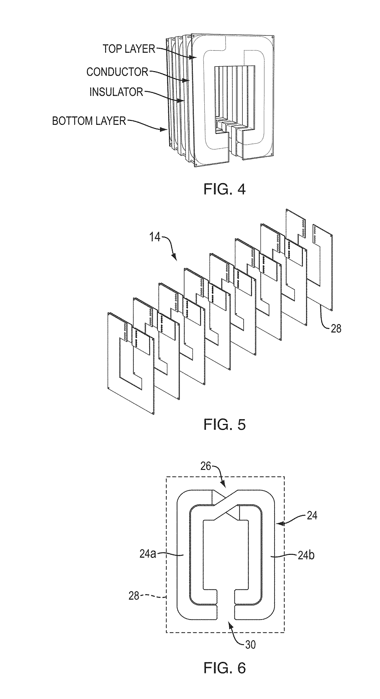
[0026]In the present invention, a high current inductor or other similar type of high current electronic device such as a transformer 10, FIG. 1, is constructed as a potted device having a magnetic core 12, FIG. 2, a planar type winding 14 (explained in greater detail below), a fluid cooling path 16 in the form of a cooling plate (for example, a cooling structure or jacket) and a thermal insulation layer 20. The component 10 is encased in an epoxy or other similar encapsulant forming “potting”22 as well known in the art.

[0027]In one embodiment, the inductor FIG. 10 is of a “shell” type core construction such that the magnetic core 12 is outside the conductor and “sandwiches” the windings 14. In this case, the core 12 is of a three legged construction with a center leg 38, FIG. 12, over which the winding 14 (having a central opening 40) fits. The inductor may also be of a core-type construction FIG. 11. Both shell type and core-type transformer constructions are well known in the art...

third embodiment

[0035]In a third embodiment, the inductor or similar device made in accordance with the teachings of the present invention may be constructed with the winding 14 created by using copper foil. The inductor may be constructed with the foil winding between two cold plates (FIG. 9) to provide cooling for the full structure.

[0036]The inductor in the third embodiment with the cold plates is attached to the windings to maintain a cooling to the outer surface and guarantee that all heat is transferred to the water including the temperature rise due to the core and gap structures.

[0037]Accordingly, the present invention provides a method to construct a high current electronic device such as an inductor or a transformer utilizing a single or multi-layer PCB with split traces or laminated bus bars and a high current electronic device built according to these methods. Traces are set-up with cross-overs to ensure the length of all traces is equal to maintain good current sharing. Then, PCBs are ...


PUM


Abstract

A method to construct a high current electronic device such as an inductor or a transformer with a single or multi-layer PCB with split traces and / or laminated bus bars and a high current electronic device built according to these methods. Traces are set-up with cross-overs to ensure the length of all traces is equal to maintain good current sharing. Then, PCBs or bus bars are stacked to provide the turns required for the inductor. Cooling plates are provided to cool the structure which is in turn encapsulated in a potting material.

Description

CROSS-REFERENCE TO RELATED APPLICATIONS[0001]This application claims priority from U.S. Provisional Patent Application No. 62 / 271,514 titled “High Current Potted Inductor And A Method Of Manufacturing Same” filed on Dec. 28, 2015 and which is incorporated fully herein by reference.TECHNICAL FIELD[0002]The present invention relates to electronic power components and more particularly, relates to high current handling devices such as high current handling power inductors or transformers that are potted in a package and constructed from a single or multi-layer PCB with split traces.BACKGROUND INFORMATION[0003]Due to the advances in power electronics and the requirements for higher power factors, more and more demand has been registered for harmonic filter inductors and DC link inductors. Furthermore, due to the introduction of switch mode topologies, many inductive components are subjected to an additional higher frequency component in addition to the lower frequency fundamental or dir...

Claims


Application Information

Patent Timeline
IPC IPC(8): H01F27/22H01F27/24H01F27/02H01F27/28H01F41/02
CPCH01F27/22H01F27/022H01F2027/2809H01F27/2804H01F41/02H01F27/24H01F27/16
Inventor BENZERROUK, SOUHEIL
Owner WARNER POWER ACQUISITION LLC
Learn More