
Edge-emitting semiconductor laser

Active Publication Date: 2017-11-30
MITSUBISHI ELECTRIC CORP
View PDF5 Cites 0 Cited by
  • Summary
  • Abstract
  • Description
  • Claims
  • Application Information

AI Technical Summary

Benefits of technology

The present invention provides an edge-emitting semiconductor laser that can prevent changes in lasing wavelength due to temperature without affecting productivity and yield. This is achieved by using a Bragg reflector with alternating layers of low-refractive-index and high-refractive-index layers between the active layer and the light absorption layer.

Problems solved by technology

Part of light having propagated through the waveguide exits to the outside through one of the semiconductor facets, thereby causing a mirror loss.
There is a problem that the distance through which an optical signal is transmitted is limited under the influence of this dispersion.
These lasers, however, have complicated structures such that processing on the order of submicrons at the time of manufacturing of the device is required, resulting in reductions in productivity and yield.

Method used


Image

  • Edge-emitting semiconductor laser
  • Edge-emitting semiconductor laser
  • Edge-emitting semiconductor laser

Examples


first embodiment

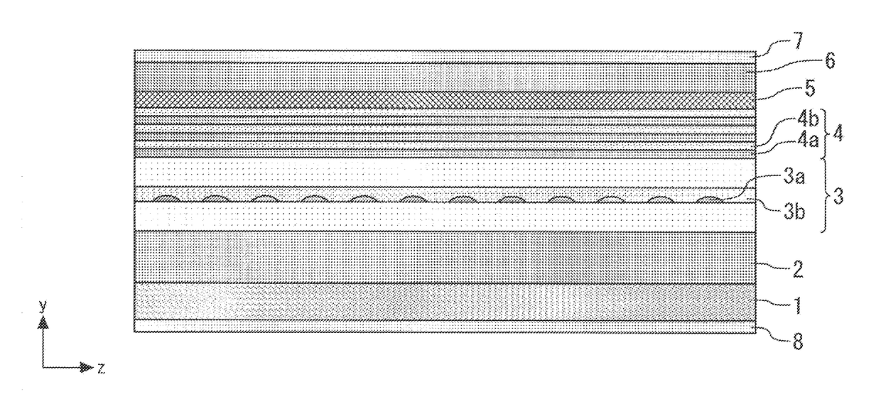
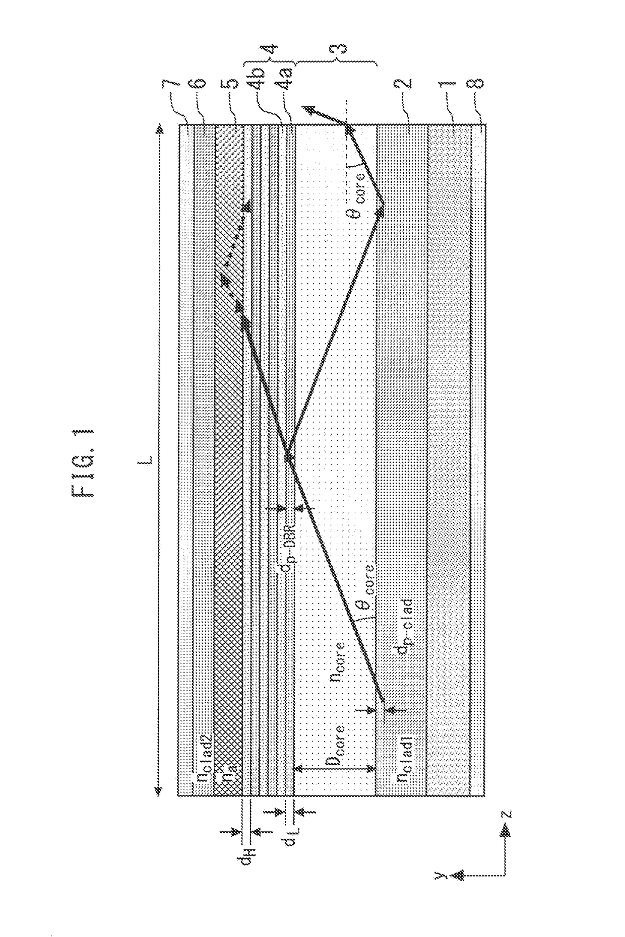
[0021]FIG. 1 is a sectional view of an edge-emitting semiconductor laser according to a first embodiment of the present invention. A first cladding layer 2 having a first refractive index nclad1 and formed of InP is fainted on an InP substrate 1. An active layer 3 having a second refractive index ncore higher than the first refractive index nclad1 is formed on the first cladding layer 2. The active layer 3 may be constituted of an InGaAsP-based or AlGaInAs-based semiconductor and may include a multiple quantum well layer. The thickness of the active layer 3 is Dcore.

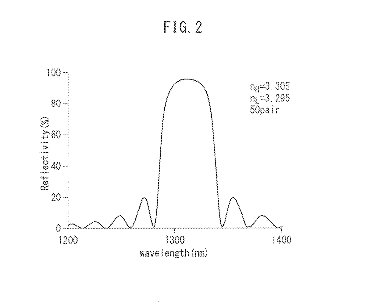
[0022]A Bragg reflector 4 (DBR) formed of an InGaAsP-based or AlGaInAs-based semiconductor is formed on the active layer 3. The Bragg reflector 4 has a periodic structure in which low-refractive-index layers 4a each having a thickness dL and a refractive index nL, and high-refractive-index layers 4b each having a thickness dH and a refractive index nH are alternately superposed one on another. These refractive indices ar...

second embodiment

[0039]FIG. 5 is a sectional view of an edge-emitting semiconductor laser according to a second embodiment of the present invention. A light absorption layer 9 is formed on the first cladding layer 2 instead of the Bragg reflector 4 and the light absorption layer 5 in the first embodiment, and a Bragg reflector 10 is formed on the light absorption layer 9. The active layer 3 is formed on the Bragg reflector 10. The Bragg reflector 10 has low-refractive-index layers 10a and high-refractive-index layers 10 each having a thickness larger than λ / 4n and alternately laid one on another, as does the Bragg reflector 4. In other respects, the arrangement is the same as that in the first embodiment. Also with the arrangement according to the present embodiment, the same effect as that in the case of the first embodiment can be obtained.

third embodiment

[0040]FIG. 6 is a sectional view of an edge-emitting semiconductor laser according to a third embodiment of the present invention. In the third embodiment, both the Bragg reflector 4 and light absorption layer 5 in the first embodiment and the Bragg reflector 10 and light absorption layer 9 in the second embodiment are provided. By providing the absorption layers and the Bragg reflectors both on the upper side and on the lower side of the active layer 3 in this way, wavelength selectivity higher than that in the first embodiment can be obtained.


PUM


Abstract

An edge-emitting semiconductor laser includes: a semiconductor substrate; a first cladding layer having a first refractive index and formed on the semiconductor substrate; an active layer formed on the first cladding layer and having a second refractive index higher than the first refractive index; a Bragg reflector formed on the active layer and in which low-refractive-index layers and high-refractive-index layers each having a thickness larger than λ / 4n are alternately laid one on another where λ is an lasing wavelength and n is a refractive index of a medium; a light absorption layer formed on the Bragg reflector and having bandgap energy lower than that of the active layer; and a second cladding layer formed on the light absorption layer and having a third refractive index lower than the second refractive index.

Description

BACKGROUND OF THE INVENTIONField[0001]The present invention relates to an edge-emitting semiconductor laser which emits light from a waveguide facet.Background[0002]In a semiconductor laser, a core layer of a high refractive index including an active layer is sandwiched between cladding layers of a low refractive index provided above and below the core layer so as to form a waveguide. One of the cladding layers between which the active layer is sandwiched is doped to be p-type while the other cladding layer is doped to be n-type. Holes injected from the p-type cladding layer side and electrons injected from the n-type cladding layer side recombine to emit light in the active layer. Part of the light produced from the active layer is totally reflected at the interface between the core layer and the cladding layer to return into the active layer. The light is given a gain and amplified during passage through the active layer and is totally reflected again at the interface between the ...

Claims


Application Information

Patent Timeline
IPC IPC(8): H01S5/125H01S5/042H01S5/34H01S5/343
CPCH01S5/125H01S5/3412H01S5/0425H01S5/34313H01S5/18H01S5/187H01S5/2022H01S5/2027H01S5/305H01S5/3213H01S2301/166
Inventor FUCHIDA, AYUMIOKUNUKI, YUICHIRO
Owner MITSUBISHI ELECTRIC CORP
Learn More