
Lead frame and method of manufacturing the same

a lead frame and manufacturing method technology, applied in the field of lead frame, can solve the problems of warping, detachment from the resin, use of two kinds of plating solution, etc., and achieve the effect of improving the adhesion to the resin and not reducing the productivity

Active Publication Date: 2011-04-21
CHANG WAH TECH
View PDF5 Cites 0 Cited by
  • Summary
  • Abstract
  • Description
  • Claims
  • Application Information

AI Technical Summary

Benefits of technology

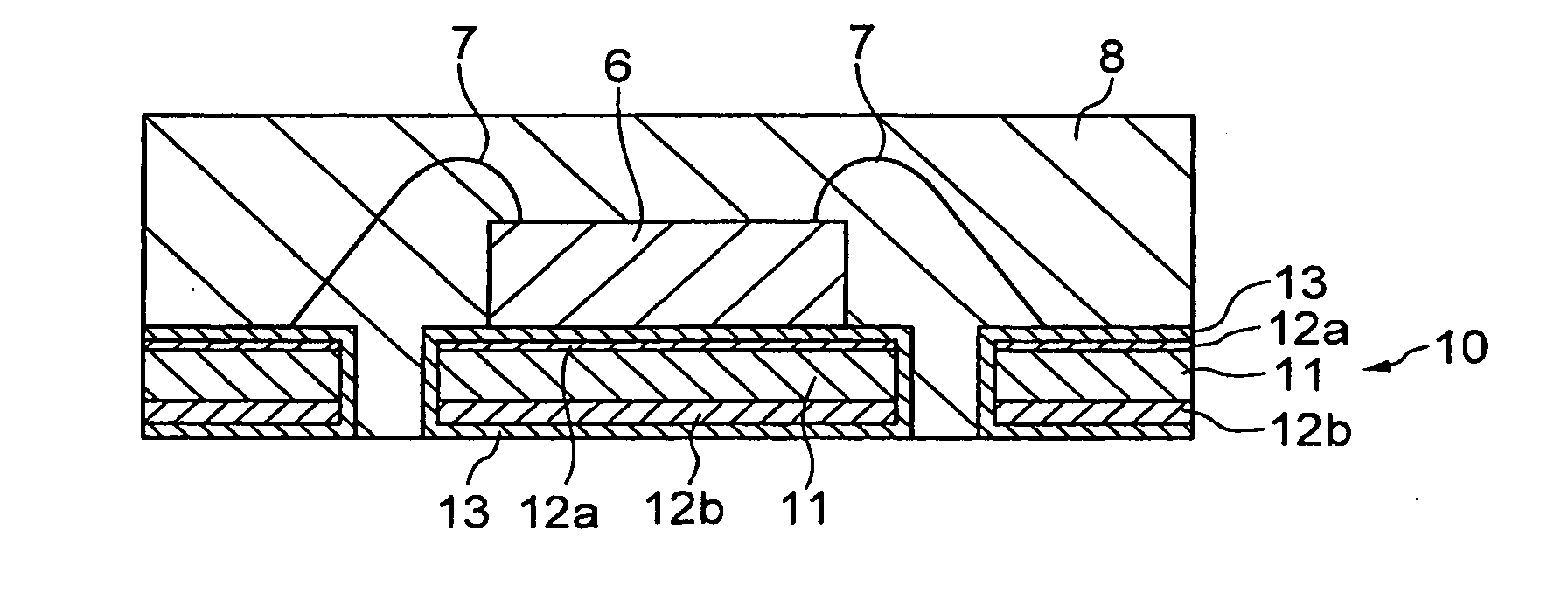
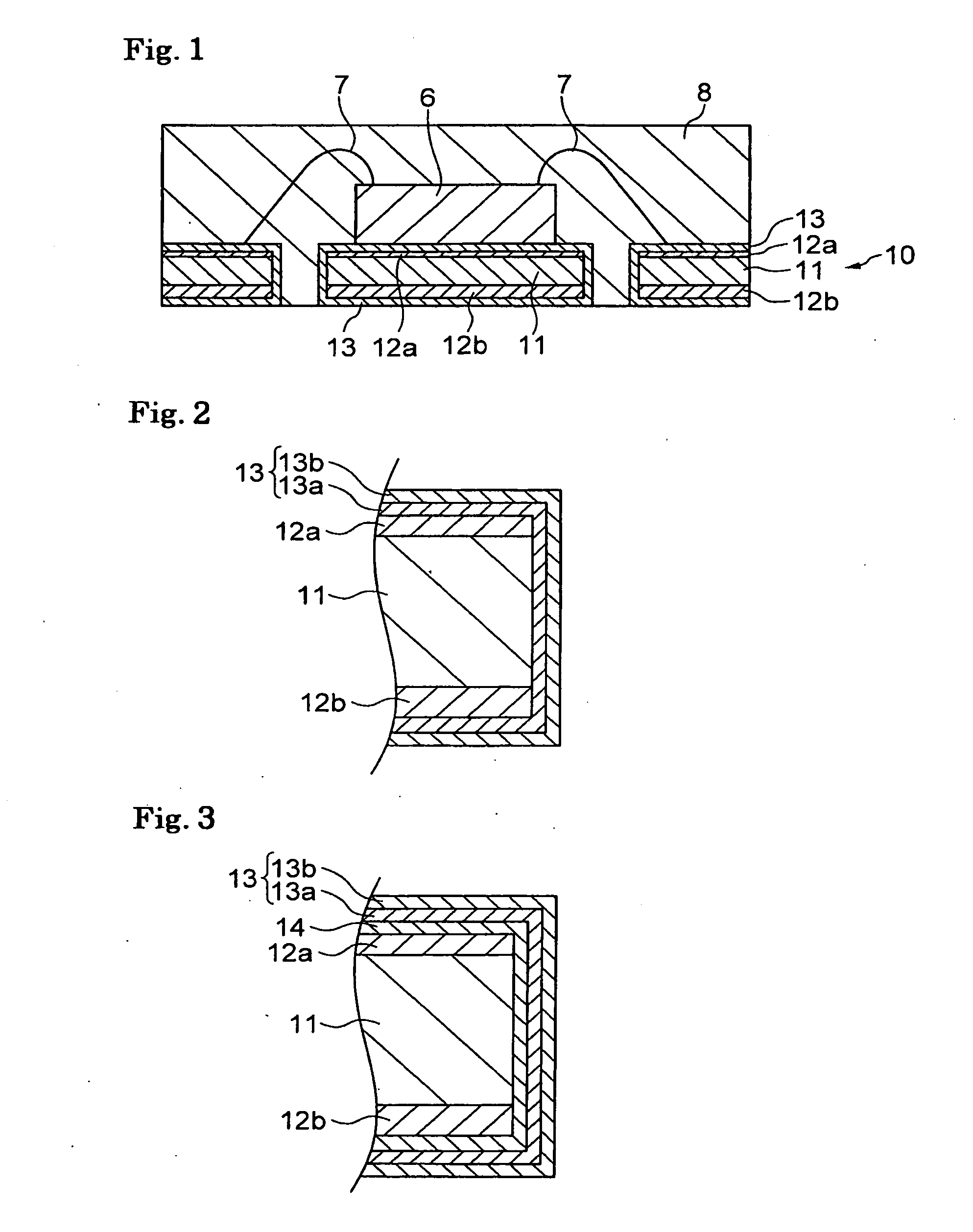
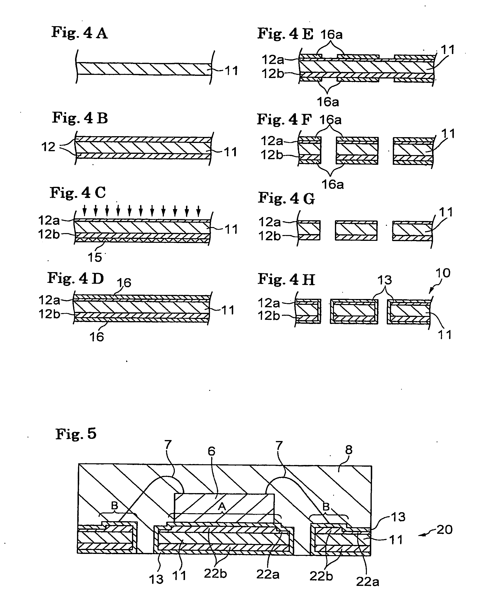
The present invention provides a lead frame with a plated layer to improve adhesion between the lead frame and the resin used for encapsulation without reducing productivity. The lead frame includes a base material with a front surface for mounting of a semiconductor chip and a back surface for connection with an external board, and an Ni layer having thick and thin sections formed on both the front and back surfaces of the base material. The thick section is formed on the back surface of the base material, and the thin section is formed on all or a part of the front surface of the base material. The lead frame may also have a Pd layer and an Au-plated layer over the thick section and the thin section, and an overhanging section having a reversed staircase shape may be formed on an edge of the die pad section and / or lead section. The method for manufacturing the lead frame includes steps of forming an Ni layer on both the front and back surfaces of the metallic base material, etching only the Ni layer on the front surface to reduce its thickness, and optionally forming a mask and etching a part of the metallic base material and the Ni layer. The lead frame has improved adhesion to the resin used for encapsulation.

Problems solved by technology

This feature however suffers from insufficient adhesion between the lead sections 5b and the resin 8, which leads to a problem in that some lead sections 5b become detached from the resin 8 and falloff during the cutting step described above.
The method of forming the Ni layers disclosed in Japanese Patent Application Laid-Open No. 2006-93559 may however cause a problem of warping due to the stress difference between the Ni layers, which are sequentially formed on each of the front and back surfaces of the lead frame using two kinds of plating solutions.
Moreover, use of the two kinds of plating solution needs longer plating apparatus and more plating steps.
Accordingly, the plating process requires complicated management and more processing time, which leads to low productivity.
The micro-etching process shown in Japanese Patent Application Laid-Open No. 2006-310397 also has a problem that the etching process requires additional etching apparatus and more processing time, which also leads to low productivity.

Method used


Image

  • Lead frame and method of manufacturing the same
  • Lead frame and method of manufacturing the same
  • Lead frame and method of manufacturing the same

Examples


first example

[0048]A metallic base material of copper sheet 0.2 mm thick and 180 mm wide was pretreated for plating. Thereafter, an Ni layer having a thickness ranging from 3.3 to 4.1 μm was formed on front and back surfaces of the metallic base material using a sulphamic acid Ni plating bath.

[0049]Next, one side (front surface side) of the metallic base material having the Ni layer was sprayed with an etching solution (ferric chloride solution) for approximately 10 seconds to reduce the thickness of the Ni layer on this side by 0.8-1.0 μm. In this manner, a thin section having a thickness ranging from 2.3 to 3.2 μm was formed.

[0050]Although no protective film using a resist was provided on the reverse side (back side) of the metallic base material, no substantial problem was observed. In other words, an absence of protective film caused no substantial problem with regard to the spreading and adhesion of the etching solution to the Ni layer on the reverse side of the metallic base material, prov...

second example

[0057]In a manner similar to that in the first example, an Ni layer having a thickness ranging from 3.0 to 3.5 μm was formed on the front and back surfaces of the metallic base material using a sulphamic acid Ni plating bath. Next, a mask was formed on the side for mounting of a semiconductor device using a resist to protect a region for placing the semiconductor device and a region for providing wire bonding. A region of the Ni layer exposed from the mask was sprayed with an etching solution for approximately 10 seconds to reduce the thickness of the exposed region by approximately 1.0 μm. The mask was then removed.

[0058]Thereafter, the steps similar to those in the first example were performed to complete fabrication of a lead frame. The characteristic of this lead frame was that the Ni layer had a thick section in the region for placing a semiconductor device (die-pad site) and the region for providing a wire bonding (wire-bonding site), and that the Ni layer had a thin section i...


PUM


Abstract

A lead frame includes a base material having a front surface for mounting of a semiconductor chip and a back surface for connection with an external board, and an Ni layer having a thick section and thin section. The thick section is formed on the back surface of the base material, whereas the thin section is formed on all or a part of the front surface of the base material. It is preferable that the thick section has a thickness ranging from 2.5 to 5 μm, and the thin section is 0.5-2 μm thinner than the thick section. The lead frame can be manufactured with improved productivity by forming an Ni layer on both front and back surfaces of the base material, and then etching only the Ni layer formed on the front surface of the base material.

Description

BACKGROUND OT THE INVENTION[0001]1. Field of the Invention[0002]The present invention relates to a lead frame and its method of manufacture, and is particularly concerned with a lead frame used for manufacturing a semiconductor package with single-sided encapsulation, such as an SON (Small Outline Non-Leaded) or a QFN (Quad Flat Non-Leaded).[0003]2. Description of the Related Art[0004]There is increasing use of chip-size packages for semiconductor devices mounted on a printed circuit board or the like due to market demand along with downsizing and miniaturization of electronic devices. In particular, a semiconductor package with single-sided encapsulation such as an SON package or a QFN package is commercially produced for semiconductor device that uses a lead frame for its manufacture. The semiconductor package with single-sided encapsulation uses resin that encapsulates or encloses a semiconductor chip or die placed on an upper surface of the lead frame, while exposing a portion o...

Claims


Application Information

Patent Timeline
Patent Type & Authority Applications(United States)
IPC IPC(8): H01L21/60
CPCH01L23/49548H01L2924/01033H01L24/48H01L2224/48091H01L2224/48247H01L2224/484H01L2224/85444H01L2924/01004H01L2924/01005H01L2924/01028H01L2924/01029H01L2924/01046H01L2924/01047H01L2924/01078H01L2924/01079H01L2924/01082H01L2924/014H01L2924/18301H01L2924/19043H01L23/49582H01L2924/01006H01L2924/00014H01L2924/181H01L2224/45099H01L2224/05599H01L2924/00012H01L23/48
Inventor MIKAMI, JUNTARO
Owner CHANG WAH TECH
Learn More