Amplifier
- Summary
- Abstract
- Description
- Claims
- Application Information
AI Technical Summary
Benefits of technology
Problems solved by technology
Method used
Image

Examples
first modification
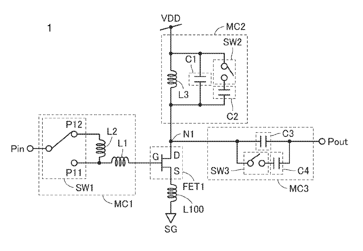
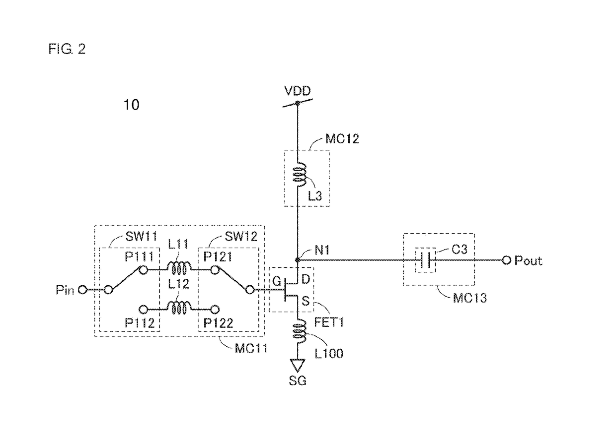
[0059]In the embodiment, reference has been made to the case where a first matching circuit can perform two-stage matching of the input impedance. In the embodiment, further reference has been made to the case where each of a second matching circuit and a third matching circuit can perform two-stage matching of the output impedance. The first matching circuit may be capable of performing three or more stage matching of the input impedance. Each of the second matching circuit and the third matching circuit may be capable of performing three or more stage matching of the output impedance. In a first modification, the first matching circuit includes three inductors to make three-stage matching of the input impedance feasible, and each of the second matching circuit and the third matching circuit includes two switches so that the second matching circuit can perform four-stage switching and the third matching circuit can perform four-stage switching. Accordingly, the following descriptio...
second modification
[0069]In the embodiment, an amplifier including one transistor has been described. Alternatively, an amplifier including more than one transistor may be used. In a second modification, two transistors are connected in cascode between the power supply and the ground point.
[0070]FIG. 12 is an exemplary circuit diagram of a low-noise amplifier 1B according to a second modification of the embodiment. In FIG. 12, the elements illustrated in FIG. 1 are not described repeatedly. As illustrated in FIG. 12, the low-noise amplifier 1B further includes a second transistor FET2 in addition to the configuration illustrated in FIG. 1. The second transistor FET2 is a field effect transistor and includes a gate, a source, and a drain. The source of the second transistor FET2 is connected to the drain of the first transistor FET1. The drain of the second transistor FET2 is connected to the node N1. A bias adjustment circuit (not illustrated) is connected to the gate of the second transistor FET2.
[00...
third modification
[0072]In the embodiment, reference has been made to the case where a transistor included in an amplifier is a field effect transistor. Alternatively, the amplifier may include a bipolar transistor. In a third modification, a description relates to a case where an amplifier includes a bipolar transistor. The difference between the third modification and the embodiment is that a transistor included in an amplifier is a bipolar transistor. Other configurations are similar and are not described repeatedly.
[0073]FIG. 13 is an exemplary circuit diagram of a low-noise amplifier 1C according to the third modification of the embodiment. In FIG. 13, the elements illustrated in FIG. 1 are not described repeatedly. As illustrated in FIG. 13, the low-noise amplifier 1C includes a first transistor BPT1, which is a bipolar transistor, in place of the first transistor FET1 illustrated in FIG. 1. The first transistor BPT1 includes a base (B) that is a control terminal, an emitter (E) that is a first...
PUM
 Abstract
Description
Claims
Application Information
 - R&D Engineer
- R&D Manager
- IP Professional
- Industry Leading Data Capabilities
- Powerful AI technology
- Patent DNA Extraction
Browse by: Latest US Patents, China's latest patents, Technical Efficacy Thesaurus, Application Domain, Technology Topic.
© 2024 PatSnap. All rights reserved.Legal|Privacy policy|Modern Slavery Act Transparency Statement|Sitemap