
Electro-optical device and electronic apparatus

a technology of electro-optical devices and electronic devices, applied in the direction of optics, cross-talk/noise/interference reduction, instruments, etc., can solve the problems of large length of routed wirings, inability to downsize electro-optical devices, and increase the number of terminals needed for packaging with high definition, so as to reduce the area used for wire routing and downsize the entire device

Active Publication Date: 2018-02-01
SEIKO EPSON CORP
View PDF3 Cites 7 Cited by
  • Summary
  • Abstract
  • Description
  • Claims
  • Application Information

AI Technical Summary

Benefits of technology

The invention provides a way to make electro-optical devices with compact, high-definition, and high-quality displays. This means that the area used for arranging the terminals and the area used for routing wirings are reduced, resulting in a more efficient and effective device.

Problems solved by technology

In an electro-optical device such as a liquid crystal panel, there is a problem that the number of terminals necessary for packaging with high definition increases.
When the number of terminals increases, there is a problem that the arrangement area of the terminals and the area used for routing of wirings are increased, therefore the electro-optical device cannot be downsized.
Also, the difference in the length of routed wirings becomes large, which may cause problems in the display quality of the electro-optical device.

Method used


Image

  • Electro-optical device and electronic apparatus
  • Electro-optical device and electronic apparatus
  • Electro-optical device and electronic apparatus

Examples


application example

3. Application Example

[0118]FIG. 16 is a diagram showing a projector 2100 according to one embodiment. The projector 2100 is an example of the electronic apparatus using the electro-optical device 1. In the projector 2100, the electro-optical device 1 is used as a light valve, and high-definition and bright display can be achieved without enlarging the device. As shown in the diagram, a lamp unit 2102 having a white light source such as a halogen lamp is provided inside the projector 2100. The projected light emitted from the lamp unit 2102 is separated into three primary colors, red (R) color, green (G) color, and blue (B) color by three mirrors 2106 and two dichroic mirrors 2108 provided inside the lamp unit 2102. The separated projection light is guided to light valves 100R, 100G, and 100B corresponding to the respective primary colors. Since the B color light has a long optical path as compared with the other R color and G color, in order to prevent the loss thereof, the light o...

modification example

4. Modification Example

[0121]The aspect of the invention is not limited to the above-described embodiments, and various modifications can be made. Several modification examples will be described below. Two or more of the modification examples below may be used in combination.

modification example 1

4-1. Modification Example 1

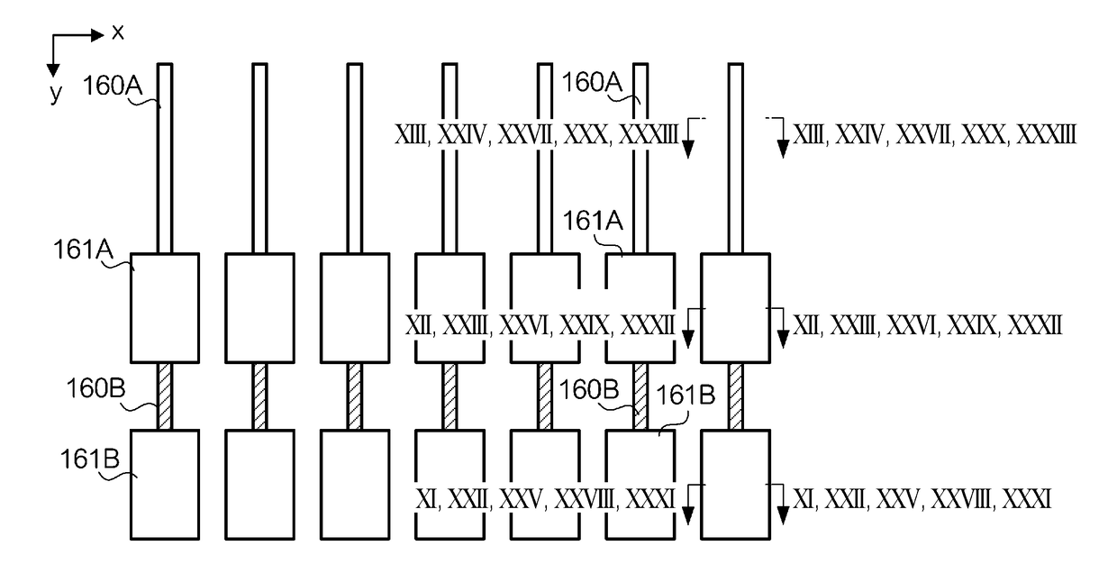
[0122]FIG. 17 is a schematic diagram showing a cross-section structure according to the modification example 1 of the video signal line 160B and the video signal input terminal 161A. The diagram shows the VIII, XVII-VIII, XVII cross section in FIG. 6 similarly to FIG. 8. The same applies to the subsequent FIGS. 18 to 20 showing a cross-section structure. In the example of FIG. 8, the pattern of the video signal input terminal 161A and the pattern of the video signal line 160B are formed in the same wiring layer (wiring layer 503). However, in the example of FIG. 17, both patterns are formed in the different wiring layers. That is, the pattern of the video signal input terminal 161A is not formed in the wiring layer 503 where the pattern of the video signal line 160B is formed. The pattern of the video signal input terminal 161A is formed on the wiring layer 504, and the pattern of the video signal line 160B is not formed. Although the video signal input te...


PUM

PropertyMeasurementUnit
distanceaaaaaaaaaa
sizeaaaaaaaaaa
sizeaaaaaaaaaa

Abstract

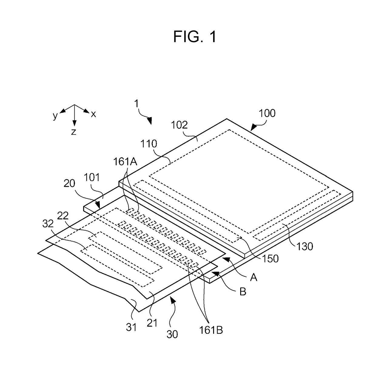
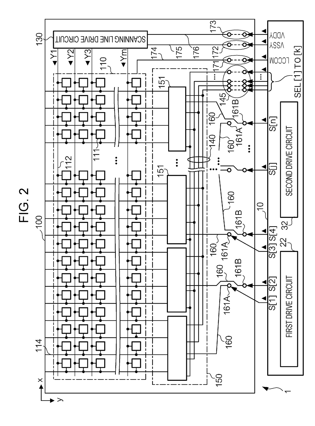
An electro-optical device includes a substrate, a first terminal that is formed on the substrate, a second terminal that is formed on the substrate and arranged in a first direction with respect to the first terminal, a third terminal that is formed on the substrate, and arranged in a second direction different from the first direction with respect to the first terminal, and of which the position in the first direction is the same as the first terminal, and a wiring that is formed on the substrate and connected to the third terminal.

Description

BACKGROUND1. Technical Field[0001]The present invention relates to an electro-optical device and an electronic apparatus.2. Related Art[0002]In an electro-optical device such as a liquid crystal panel, there is a problem that the number of terminals necessary for packaging with high definition increases. On the other hand, in JP-A-2009-194058, a technique of arranging electrode pad portions in a zigzag manner is disclosed.[0003]In recent years, with the high resolution of an electro-optical device, the number of terminals used for packaging tends to increase. When the number of terminals increases, there is a problem that the arrangement area of the terminals and the area used for routing of wirings are increased, therefore the electro-optical device cannot be downsized. Also, the difference in the length of routed wirings becomes large, which may cause problems in the display quality of the electro-optical device.SUMMARY[0004]An advantage of some aspects of the invention is to prov...

Claims


Application Information

Patent Timeline
Patent Type & Authority Applications(United States)
IPC IPC(8): G02F1/1345G02F1/1362H05K1/14H05K1/11H05K1/02
CPCG02F1/13452H05K1/111H05K1/0219H05K2201/10136G02F1/136286H05K2201/049H05K1/144G02F1/1345G02F1/13458
Inventor MASUI, JUNICHIMIYASHITA, TOMOAKI
Owner SEIKO EPSON CORP
Learn More