Iii-nitride LED with tunnel junction

a technology of nitride led and tunnel junction, which is applied in the direction of basic electric elements, electrical apparatus, and semiconductor devices, can solve the problems of low crystalline quality, large amount of impurities present, and poor control of material quality, and achieves easy scaling to large wafer diameters and throughputs, and low cost.

Active Publication Date: 2018-02-15
KORRUS INC
View PDF1 Cites 10 Cited by
  • Summary
  • Abstract
  • Description
  • Claims
  • Application Information

AI Technical Summary

Benefits of technology

[0010]Applicants have developed an approach for manufacturing a high-quality hybrid GaN tunnel junction (TJ), which is inexpensive, robust, and readily scalable to large wafer diameters and throughputs. In particular, Applicants recognize that by combining h...

Problems solved by technology

Typically, sputtering is very inexpensive and can deposit very large amounts of materials on large-area substrates; however the material quality is not very well controlled (since this is typically not a high-vacuum process).
Therefore, a large amount of impurities can be present, and sputtered material may be amorphous or semi-amorphous, with low crystalline quality.
Therefore, it is commonly thought ...

Method used


Image

  • Iii-nitride LED with tunnel junction
  • Iii-nitride LED with tunnel junction
  • Iii-nitride LED with tunnel junction

Examples


Embodiment Construction

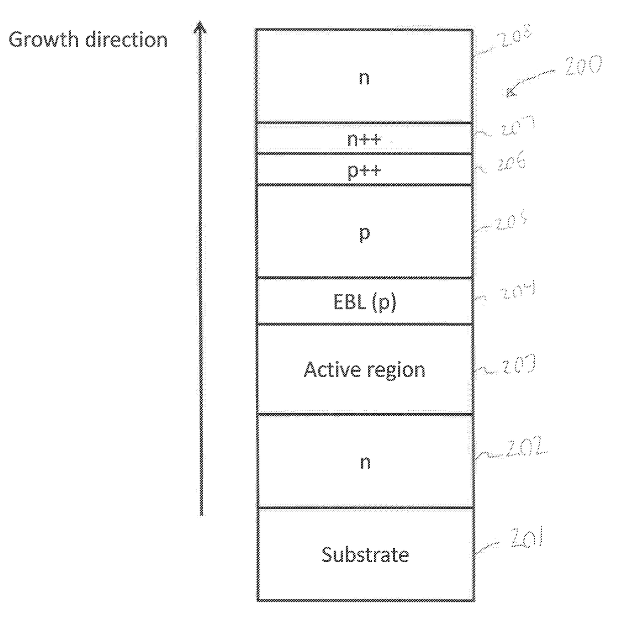
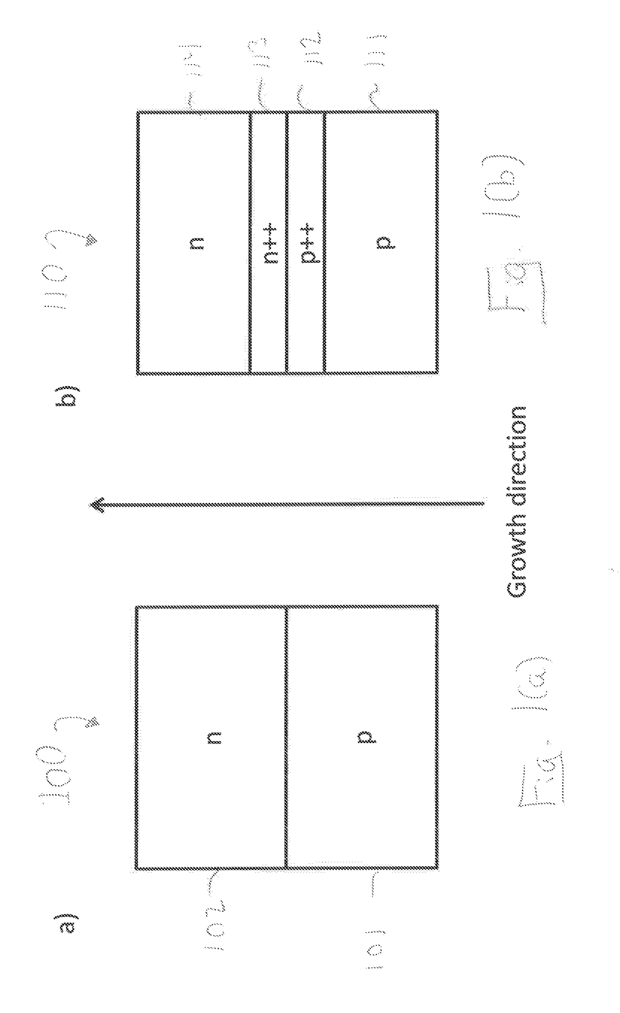
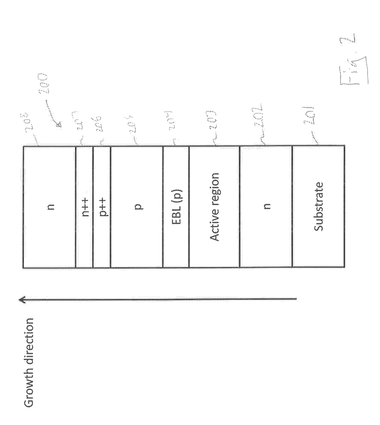
[0025]In one embodiment, the invention provides a III-Nitride optoelectronic device (including an LED, a laser diode or an electronic device) with a hybrid TJ, which features device layers grown by MOCVD and epitaxial TJ layers grown by sputtering. In a variety of embodiments, this is achieved by growing device layers in MOCVD, interrupting the growth, transferring the wafer or sample to the sputtering tool, and growing the TJ or part of the TJ by sputtering. In some embodiments, as will be discussed further, subsequent growth in MOCVD or stacks of MOCVD / sputtered layers are possible.

[0026]As used herein, “device layers” refer to layers in which an essential function of the device is performed—including a non-trivial carrier transport or light emission function. For instance, in the case of an LED, the device layers may be the light-emitting layers (also called active region), or more broadly a stack comprising the light-emitting layers and related layers (for instance: quantum well...


PUM


Abstract

A method of forming a HI-Nitride based device comprising: (a) depositing first layers by MOCVD on a substrate, wherein the first layers comprise device layers of III-Nitride material; and (b) depositing epitaxial second layers over the first layers by at least one of sputtering, plasma deposition, pulsed laser deposition, or liquid phase epitaxy, wherein the second layers comprise III-Nitride material and define at least partially a tunnel junction.

Description

REFERENCE TO RELATED APPLICATION[0001]This application is based on U.S. Provisional Application No. 62 / 372,935, filed Aug. 10, 2016, hereby incorporated by reference.FIELD OF INVENTION[0002]The invention relates generally to an optoelectric device having a tunnel junction, and, more specifically, to an optoelectric device, such as a light emitting diode LED, having a tunnel junction prepared using hybrid manufacturing techniques to optimize the device and overlaying epitaxial layers.BACKGROUND[0003]Prior art references recognize that tunnel junctions (TJs) can be useful in a variety of semiconductor devices, including GaN-based devices. Typically, standard GaN epitaxial growth ends with a p-contact; therefore, typical GaN TJs are p-to-n TJs.[0004]However, actually forming a TJ on a GaN device can be challenging. In particular, the preferred method for GaN device epitaxy is metalorganic chemical vapor deposition (MOCVD). However, MOCVD may not be ideally suited for GaN-based TJs. P-G...

Claims


Application Information

Patent Timeline
IPC IPC(8): H01L33/06H01L33/32H01L33/08H01L33/14H01L33/00H01L33/02
CPCH01L33/06H01L33/007H01L33/32H01L33/08H01L33/145H01L33/025H01L33/04
Inventor DAVID, AURELIEN J.F.D'EVELYN, MARK P.HURNI, CHRISTOPHE A.YOUNG, NATHANCICH, MICHAEL J.
Owner KORRUS INC
Why Eureka
Try Eureka