Display device and manufacturing method thereof

a technology for display devices and manufacturing methods, applied in semiconductor devices, instruments, electrical devices, etc., can solve the problems of easy deterioration of light-emitting elements containing organic compounds as their main components, partial decrease of etc., and achieve the effect of reducing the luminance of display devices and easy deterioration

Active Publication Date: 2018-02-15
SEMICON ENERGY LAB CO LTD
View PDF0 Cites 6 Cited by
  • Summary
  • Abstract
  • Description
  • Claims
  • Application Information

AI Technical Summary

Benefits of technology

[0011]In particular, a light-emitting element that contains an organic compound as its main component easily deteriorates mainly because of water. This might result in a partial decrease in the luminance of a display device. A non-light-emitting region might be formed in the display device.

Problems solved by technology

In particular, a light-emitting element that contains an organic compound as its main component easily deteriorates mainly because of water.
This might result in a partial decrease in the luminance of a display device.

Method used


Image

  • Display device and manufacturing method thereof
  • Display device and manufacturing method thereof
  • Display device and manufacturing method thereof

Examples


embodiment 1

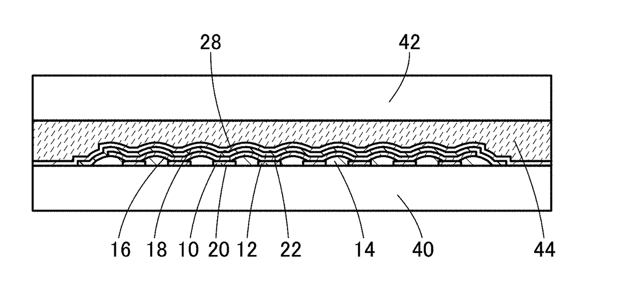
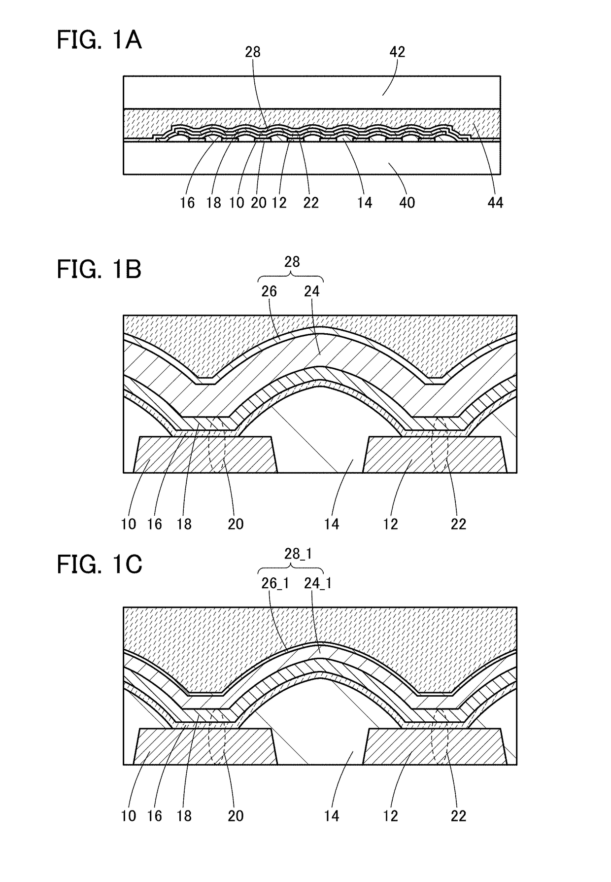
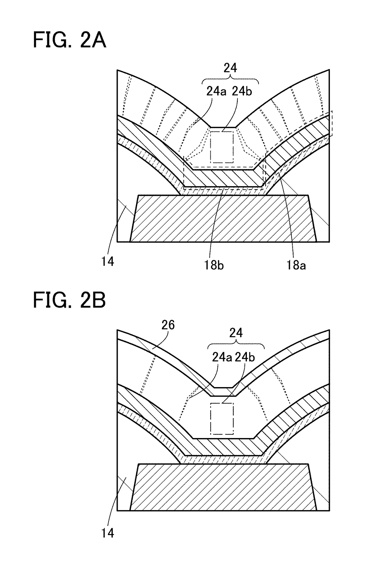
[0063]In this embodiment, an example of a display device is described with reference to FIGS. 1A to 1C and FIGS. 2A and 2B.

[0064]FIG. 1A is a schematic cross-sectional view of a display device according to this embodiment. A light-emitting element 20 and a light-emitting element 22 are positioned between a substrate 40 and a substrate 42. The light-emitting element 20 includes a first electrode 10, an EL layer 16, and a second electrode 18. The light-emitting element 22 includes a first electrode 12, the EL layer 16, and the second electrode 18. An insulating film 14 covering edge portions of the first electrodes 10 and 12 is formed. A protective film 28 is provided over the light-emitting element 20. The protective film 28 and the substrate 42 are fixed to each other with an adhesive 44. Note that the substrates 40 and 42, the adhesive 44, the first electrodes 10 and 12, the EL layer 16, the second electrode 18, and the insulating film 14 are described in detail in another embodime...

embodiment 2

[0085]In this embodiment, another structure of a display device is described with reference to FIGS. 3A and 3B. FIG. 3A is a schematic cross-sectional view of a display device according to this embodiment. The display device illustrated in FIGS. 3A and 3B is characterized by including a color film 30 and a color film 32 between the protective film 28 and the adhesive 44.

[0086]The vicinity of the light-emitting elements 20 and 22 is described with reference to an enlarged cross-sectional view illustrated in FIG. 3B. The color films 30 and 32 are provided over the protective film 28. The color film 30 overlaps with the light-emitting element 20 with the protective film 28 interposed therebetween. The color film 32 overlaps with the light-emitting element 22 with the protective film 28 interposed therebetween.

[0087]The details of the color films 30 and 32 will be described later in another embodiment.

[0088]The color films 30 and 32 can be formed by applying a composition onto the prote...

embodiment 3

[0093]In this embodiment, an example of the display device of one embodiment of the present invention will be described.

[0094]A more specific structure example of the display device of one embodiment of the present invention is described below with reference to drawings.

[0095]FIG. 4 is a perspective view of a display device 710.

[0096]The display device 710 includes a substrate 751a and a substrate 752a. In FIG. 4, the outline of the substrate 752a is illustrated by dashed lines.

[0097]The display device 710 includes a display portion 761a, a circuit portion 762a, a wiring 765a, and the like between the substrates 751a and 752a. An IC 764a and an FPC 763a are mounted on the substrate 751a. Therefore, the display device 710 can also be referred to as a display module.

[0098]In the circuit portion 762a, a circuit functioning as a scan line driver circuit can be used, for example.

[0099]The wiring 765a has a function of supplying a signal and electric power to the display portion 761a or t...


PUM

PropertyMeasurementUnit
sizeaaaaaaaaaa
thicknessaaaaaaaaaa
thicknessaaaaaaaaaa

Abstract

A highly reliable display device or electronic device is provided. The display device includes a first electrode, a second electrode, a light-emitting layer between the first electrode and the second electrode, and a protective film over the second electrode. The protective film includes a first insulating film and a second insulating film over the first insulating film. The first insulating film includes one or more of aluminum oxide, hafnium oxide, and zirconium oxide, and the second insulating film includes one or more of aluminum oxide, hafnium oxide, and zirconium oxide. A composition of the first insulating film is different from a composition of the second insulating film. A water vapor transmission rate of the protective film is lower than 1×10⁻² g/(m2·day).

Description

BACKGROUND OF THE INVENTION1. Field of the Invention[0001]One embodiment of the present invention relates to a display device. One embodiment of the present invention relates to a method for manufacturing a display device.[0002]Note that one embodiment of the present invention is not limited to the above technical field. For example, one embodiment of the present invention relates to an object, a method, or a manufacturing method. One embodiment of the present invention relates to a process, a machine, manufacture, or a composition of matter. One embodiment of the present invention relates to a memory device, a processor, a driving method thereof, or a manufacturing method thereof.[0003]Note that in this specification and the like, a semiconductor device generally means a device that can function by utilizing semiconductor characteristics. Thus, a semiconductor element such as a transistor or a diode and a semiconductor circuit are semiconductor devices. A display device, a light-em...

Claims


Application Information

Patent Timeline
Patent Type & Authority Applications(United States)
IPC IPC(8): H01L51/56H01L27/12G02F1/1368
CPCH01L51/56G02F1/1368H01L29/66007H01L51/5253H01L27/1214G02F2201/44H10K59/50H10K59/38H10K50/844H10K71/00
Inventor TSUDA, KAZUKIYOKOYAMA, KOHEIJINBO, YASUHIRO
Owner SEMICON ENERGY LAB CO LTD
Why Eureka
Try Eureka