Touch sensor and touch screen

a touch sensor and touch screen technology, applied in static indicating devices, instruments, solid-state devices, etc., can solve the problems of touch detection accuracy deterioration and the signal-to-noise ratio (sn ratio) decline, so as to improve the touch detection accuracy and reduce the sn ratio

Active Publication Date: 2018-03-01
JAPAN DISPLAY INC
View PDF16 Cites 44 Cited by
  • Summary
  • Abstract
  • Description
  • Claims
  • Application Information

AI Technical Summary

Benefits of technology

[0007]For example, in a touch screen, the touch sensor produced using a transparent substrate, a transparent conductive film, and the like is disposed on a display surface of a display panel. Therefore, a potential of the detecting electrode of the touch sensor varies due to a driving signal of the display panel and the SN ratio may decrease.
[0008]The invention provides a touch sensor which is not easily affected by electromagnetic noise from a rear surface side and achieves improvement of the touch detection accuracy in a touch screen.

Problems solved by technology

In a case in which a touch sensor is used in combination with other devices, there is a problem in that the touch sensor is likely to catch electromagnetic noise, which is caused by electric signals in the other devices, at detecting electrodes, a signal-to-noise ratio (SN ratio) decreases, and the touch detection accuracy may be deteriorated.

Method used


Image

  • Touch sensor and touch screen
  • Touch sensor and touch screen
  • Touch sensor and touch screen

Examples


first embodiment

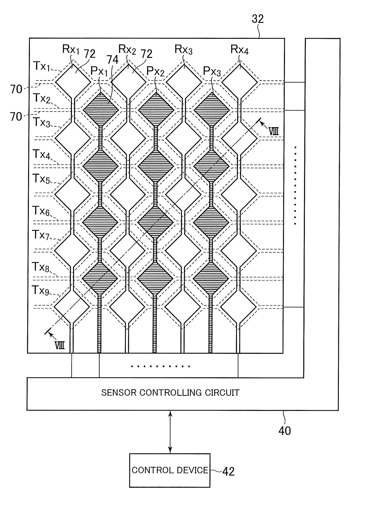
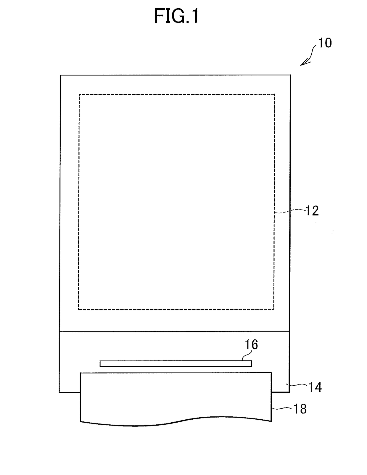
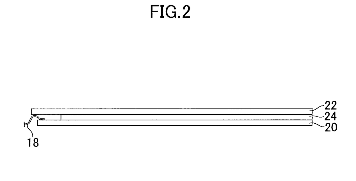
[0029]FIG. 1 is a schematic plan view of an organic electroluminescence (EL) display device according to the embodiment. The display device illustrated in FIG. 1 is a touch screen 10 in which a touch sensor is stacked on a display panel, and structures such as a light emitting element and a sensor are formed on a rectangular array substrate. On a display region 12 of the touch screen 10, a pixel array portion in which pixels including organic light emitting diodes (OLED) which are self light emitting elements are arranged is provided, and an image is displayed. Also, the touch sensor is stacked on a display surface side of the display region 12, and detects approaching and touching of a finger or the like of a user to the display surface or a position thereof. A component mounting region 14 is provided on one side of the array substrate, and a wiring connected to the display region 12 is disposed. Further, a driver IC 16 constituting a driving unit is mounted on, or a flexible print...

second embodiment

[0082]A second embodiment of the invention will be described by focusing on differences from the first embodiment described above. FIG. 11 is a schematic partial plan view illustrating patterns of the electrodes Tx, Rx, and Px in the touch screen relating to the second embodiment, and FIG. 12 is a schematic partial sectional view of the touch screen taken along line XII-XII of FIG. 11. A main difference of the second embodiment from the first embodiment is that a length of one side of an approximate rhombus shape of each of the pad electrode portions 70a of the electrodes Tx is twice a length of one side of each of the pad electrode portions 72a and 74a of the electrodes Rx and Px. The pad electrode portion 70a is approximately a rhombus shape same as that of the pad electrode portion 70a of the first embodiment, an area thereof is approximately four times, and two of the pad electrode portions 72a and 74a are disposed to face one of the pad electrode portions 70a.

[0083]Specificall...


PUM


Abstract

A touch sensor includes first electrodes which are driving electrodes of the touch sensor, second electrodes which are detecting electrodes of the touch sensor, third electrodes, and an insulating film which is stacked on the first electrodes. Each of the first electrodes extends in a first direction. Each of the second electrodes and each of the third electrodes are formed on the insulating film, and extend in a second direction. The second electrodes overlap with partial regions of the first electrodes, and the third electrodes overlap with other partial regions of the first electrodes and are formed in gaps between the second electrodes. A film thickness of the insulating film between the first electrodes and the third electrodes varies due to pressing force in a film thickness direction, and the insulating film constitutes the electrostatic capacitance-type pressure sensor with first electrodes and the third electrodes.

Description

CROSS-REFERENCE TO RELATED APPLICATION[0001]The present application claims priority from Japanese application JP2016-170044 filed on Aug. 31, 2016, the content of which is hereby incorporated by reference into this application.BACKGROUND OF THE INVENTION1. Field of the Invention[0002]The present invention relates to a touch sensor and a touch screen which is a display device provided with the touch sensor.2. Description of the Related Art[0003]As an input unit in an electronic device in recent times, a touch operation in which a subject is selected by directly touching a screen with a finger or a pointing device is widely performed, and a touch sensor for detecting the touched coordinates is provided in such an electronic device. FIG. 15 is a schematic plan view illustrating an example of an electrode structure of a projection electrostatic capacitance-type touch sensor of the related art. A touch sensor 1 illustrated in FIG. 15 is used for a touch screen and the like.[0004]The touc...

Claims


Application Information

Patent Timeline
Patent Type & Authority Applications(United States)
IPC IPC(8): G06F3/041G06F3/044H01L51/52H01L27/32
CPCG06F3/0418G06F3/044G06F3/0412H01L51/5253H01L27/323H01L27/3276G09G3/3266G09G2330/021G09G2310/08G09G3/3258G09G2300/0426G06F2203/04105G06F3/0446G06F3/0447G06F3/0445H10K59/40H10K50/844H10K59/131
Inventor MA, CHUNCHE
Owner JAPAN DISPLAY INC
Why Eureka
Try Eureka