

Minimizing Tin Loss During Thermal Processing of Kesterite Films
a technology of kesterite film and thermal processing, which is applied in the field of kesterite film, can solve the problems of limiting the performance of this technology, and achieve the effect of minimizing the loss of volatile components
- Summary
- Abstract
- Description
- Claims
- Application Information
AI Technical Summary
Benefits of technology
Problems solved by technology
Method used
Image

Examples
Embodiment Construction
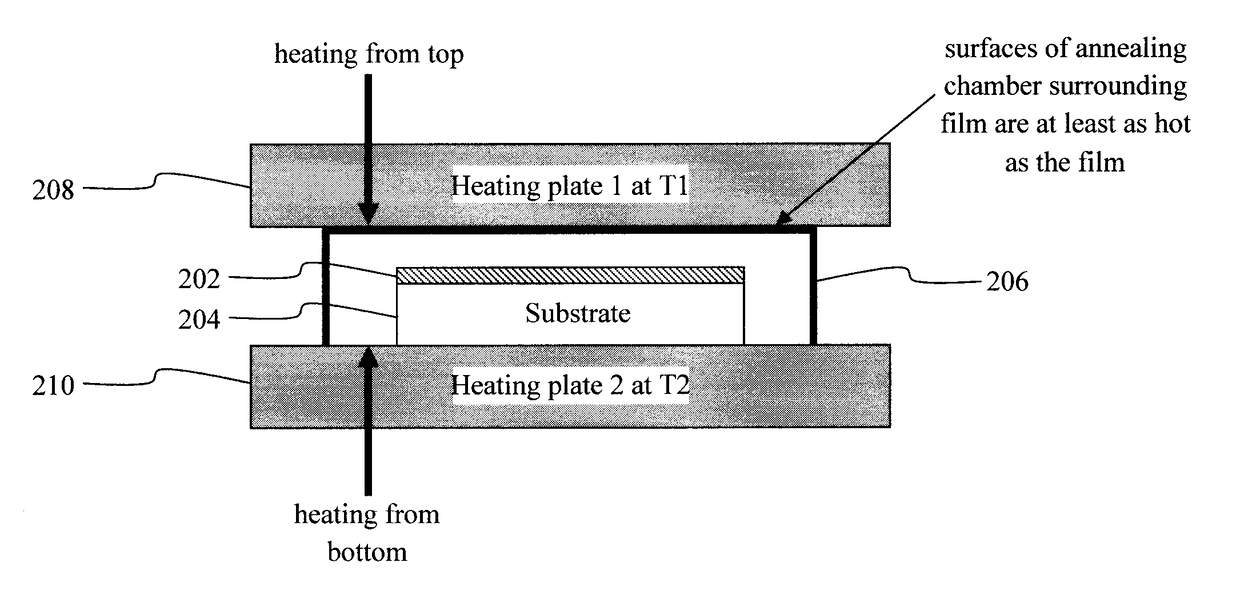
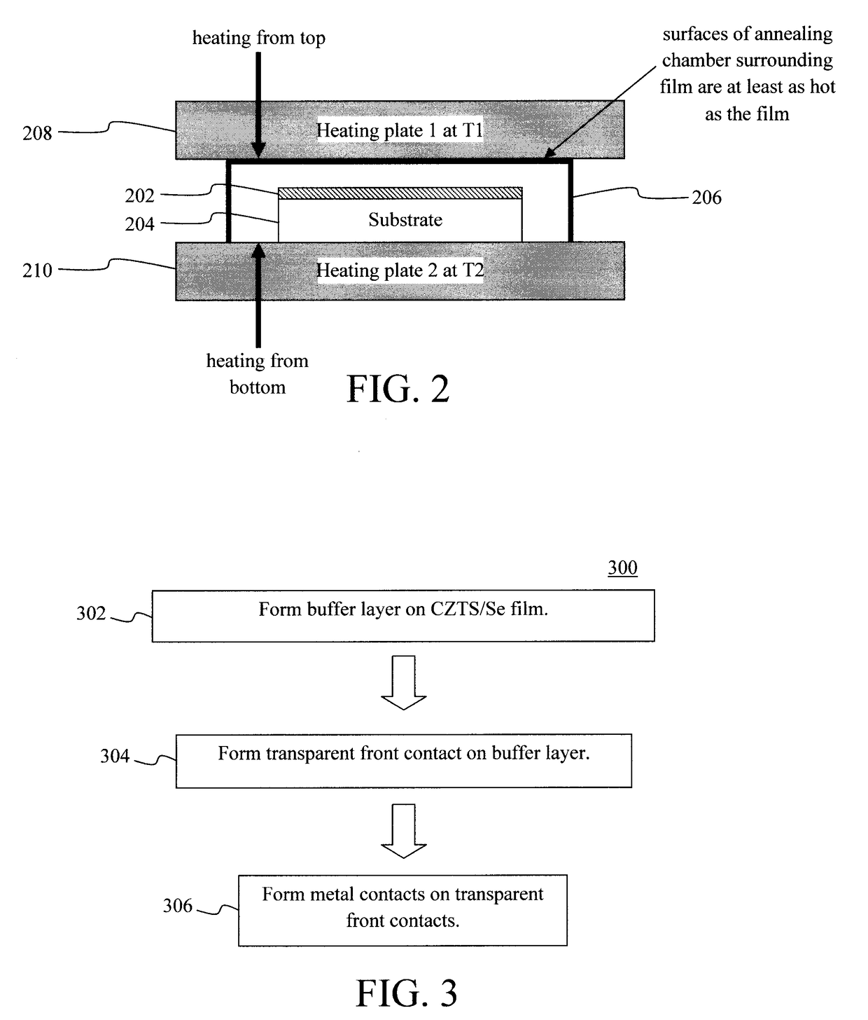
[0035]As provided above, the loss of volatile components, such as tin (Sn), during annealing of kesterite materials such as CZTS / Se presents a notable challenge for large-scale implementation of these materials. The term “CZTS / Se” as used herein refers to materials containing copper (Cu), zinc (Zn), tin (Sn), and at least one of sulfur (S) and selenium (Se). Advantageously, it has been determined herein that a major contributor to Sn loss during annealing is the condensation of volatile Sn species on cooler surfaces. However, if all of the surfaces proximate to the film are kept at a temperature that is greater than or equal to the temperature of the film, then the volatile Sn species will be directed back to the film since they will not condense on a hotter surface. Further, it is found herein that the majority of Sn is lost from the surface of the film. Thus, according to an exemplary embodiment, surfaces proximate to the surface of the film are maintained at a temperature that is...
PUM
| Property | Measurement | Unit |
|---|---|---|
| temperature T2 | aaaaa | aaaaa |
| temperature T2 | aaaaa | aaaaa |
| temperature | aaaaa | aaaaa |
Abstract
Description
Claims
Application Information