Organic light emitting diode structure

a light-emitting diode and organic technology, applied in the direction of basic electric elements, semiconductor devices, electrical equipment, etc., can solve the problems of limited efficiency of oled, inefficiency of light extraction, and limited improvement in relation to oled efficiency, so as to suppress the propagation of surface plasmon polaritons

Active Publication Date: 2018-03-22
LOMOX
View PDF3 Cites 5 Cited by
  • Summary
  • Abstract
  • Description
  • Claims
  • Application Information

AI Technical Summary

Benefits of technology

[0016]In a first aspect there is provided an organic light emitting diode (OLED) having an organic electroluminescent layer formed between a first electrode and a second electrode. One of the first and second electrodes is a transparent electrode having a surface through which light is emitted from the OLED to the outside. The transparent electrode has a plasmonic photonic crystal structure fabricated having an artificial lattice with a pitch in density variation intermediate in size between a metallic crystal and a photonic crystal formed in the same material as the transparent electrode, thereby operable to suppress propagation of the surface plasmon polaritons at the surface.

Problems solved by technology

However, whilst efficient in comparison to LCDs and PDPs, the efficiency of the OLED is limited, due to incomplete light extraction from the active, light-emitting layer due to losses in the OLED.
Whilst the HIL, HTL, ETL, and HBL address the electrical efficiency of OLEDs, one of the key challenges in the design of OLEDs is to optimize their light extraction efficiency.
For conventional OLEDs as depicted in FIG. 1, light extraction inefficiencies exist because light generated within a high-index organic material has difficulty propagating into the surrounding lower-index Anode / Glass substrate owing to total internal refection (TIR) at the glass / air interface, coupling to dielectric waveguide modes of the organic layers, in-plane emission, and dissipation into the metal contacts of the OLED.
However, using these methods, the improvement in relation to OLED efficiency is limited.
Moreover, some of these methods have disadvantages associated with them such as a reduction in electrical efficiency, a decrease in lifetime, a viewing angle dependent colour, complicated fabrication processes and high costs.
For instance, eliminating TIR using antireflective coatings does not work as each of the layers will refract the light and ultimately the final interface with air will still meet the TIR condition.
In addition, establishing gratings at pitches less than half the UV exposure wavelength is very difficult.

Method used


Image

  • Organic light emitting diode structure
  • Organic light emitting diode structure
  • Organic light emitting diode structure

Examples


first embodiment

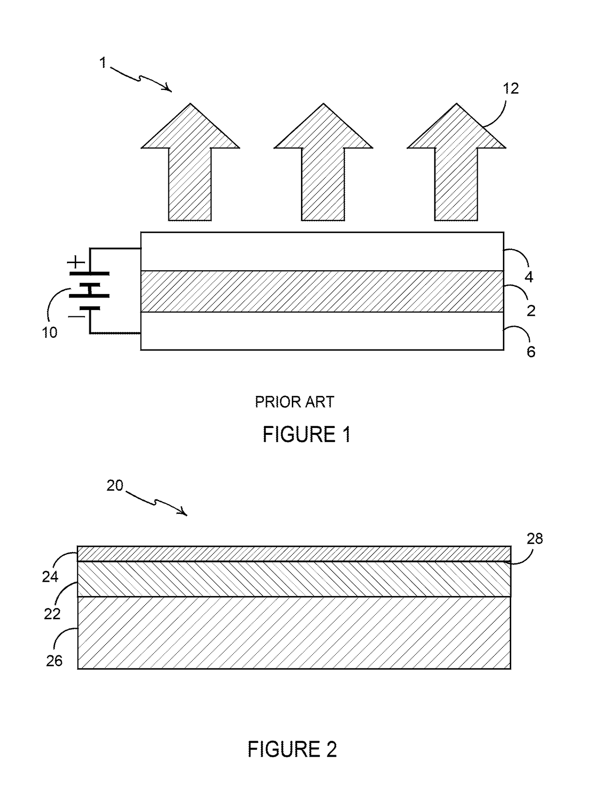
[0040]FIG. 2 shows in section, an OLED 20 according to the present invention, whereby an organic electroluminescent material layer 22 is located between two electrodes; an anode 24 and a reflecting cathode 26. As detailed above HIL, HTL, ETL and / or an HBL layer could also be used in the OLED 20 to improve electrical efficiency as required.

[0041]The anode 24 is fabricated as a plasmonic metallic photonic crystal (PC) layer and is transparent and has a surface through which light is emitted from the OLED 20 to the outside. In this case, the PC layer is a 1-100 nm silver (Ag) layer, but the PC layer may be fabricated of any suitable material as will become apparent to a skilled person having read this specification, e.g., aluminium (Al), gold (Au), etc. As above the cathode 26 may be fabricated from any suitable material (e.g., magnesium-silver or lithium-aluminium alloy).

[0042]It is known that metals conduct electricity because electrons in the metal are generally free to propagate th...

second embodiment

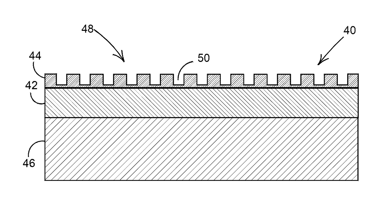
[0062]FIG. 4 shows in section, an OLED 40 according to the present invention, whereby an organic electroluminescent material layer 42 is located between two electrodes; an anode 44 and a reflecting cathode 46. As detailed above HIL, HTL, ETL and / or HBL could also be used in the OLED 40 to improve electrical efficiency as required.

[0063]The anode 44 is fabricated as a plasmonic metallic photonic crystal (PC) layer and is transparent and has a surface through which light is emitted from the OLED 40 to the outside. In the present embodiment the PC layer is a silver (Ag) layer with depth dA having at least one grating formation 48 comprising a regularly repeating periodic structure formed therein.

[0064]Although fabricated of evaporated silver in the present embodiment, the anode 44 may be fabricated of any suitable material using any suitable technique as will become apparent to a skilled person having read this specification, e.g., gold (Au), aluminium (Al), etc. Furthermore, the catho...


PUM


Abstract

An organic light emitting diode (OLED) having an organic electroluminescent layer formed between a first electrode and a second electrode. One of the first and second electrodes is a transparent electrode having a surface through which light is emitted from the OLED to the outside. The transparent electrode has a plasmonic photonic crystal structure fabricated having an artificial lattice with a pitch in density variation intermediate in size between a metallic crystal and a photonic crystal formed in the same material as the transparent electrode, thereby operable to suppress propagation of the surface plasmon polaritons at the surface.

Description

CROSS REFERENCE TO RELATED APPLICATIONS[0001]This is a division patent application of co-pending U.S. patent application Ser. No. 14 / 894,667, filed Nov. 30, 2015. The contents of this prior application are incorporated herein by reference.BACKGROUND OF THE INVENTION[0002]This invention relates to electroluminescent devices and in particular to electroluminescent devices based on organic light emitting diodes (OLEDS).[0003]Known organic light-emitting diodes (OLEDs) generally comprise an emissive electroluminescent organic semiconductor material layer formed between a cathode and an anode formed on a glass substrate, whereby the electroluminescent organic semiconductor material emits light when a voltage is applied across the anode and cathode electrodes.[0004]In order for visible light to be emitted from the OLED, at least one of the electrodes must be transparent to radiation in the 350 nm-800 nm wavelength range.[0005]OLEDs are considered to be suitable candidates for the next gen...

Claims


Application Information

Patent Timeline
Patent Type & Authority Applications(United States)
IPC IPC(8): H01L51/52
CPCH01L51/5209H01L51/5218H01L51/5265H10K50/82H10K50/818H10K50/852H10K50/813
Inventor COPNER, NIGEL JOSEPH
Owner LOMOX
Why Eureka
Try Eureka