Semiconductor device

Active Publication Date: 2018-03-29
ABLIC INC
View PDF1 Cites 0 Cited by
  • Summary
  • Abstract
  • Description
  • Claims
  • Application Information

AI Technical Summary

Benefits of technology

[0027]In the ESD protection element configured to protect a semiconductor device that is high in withstanding voltage from noise or a surge, the first N-type low concentration diffusion layer is formed, as an offset layer for easing the electric field concentration, under the LOCOS oxide film formed at each end of the gate electrode, and the second N-type low concentration diffusion layer and the third low concentration diffusion layer a

Problems solved by technology

The existing methods, however, lead to an i

Method used


Image

  • Semiconductor device
  • Semiconductor device
  • Semiconductor device

Examples


Embodiment Construction

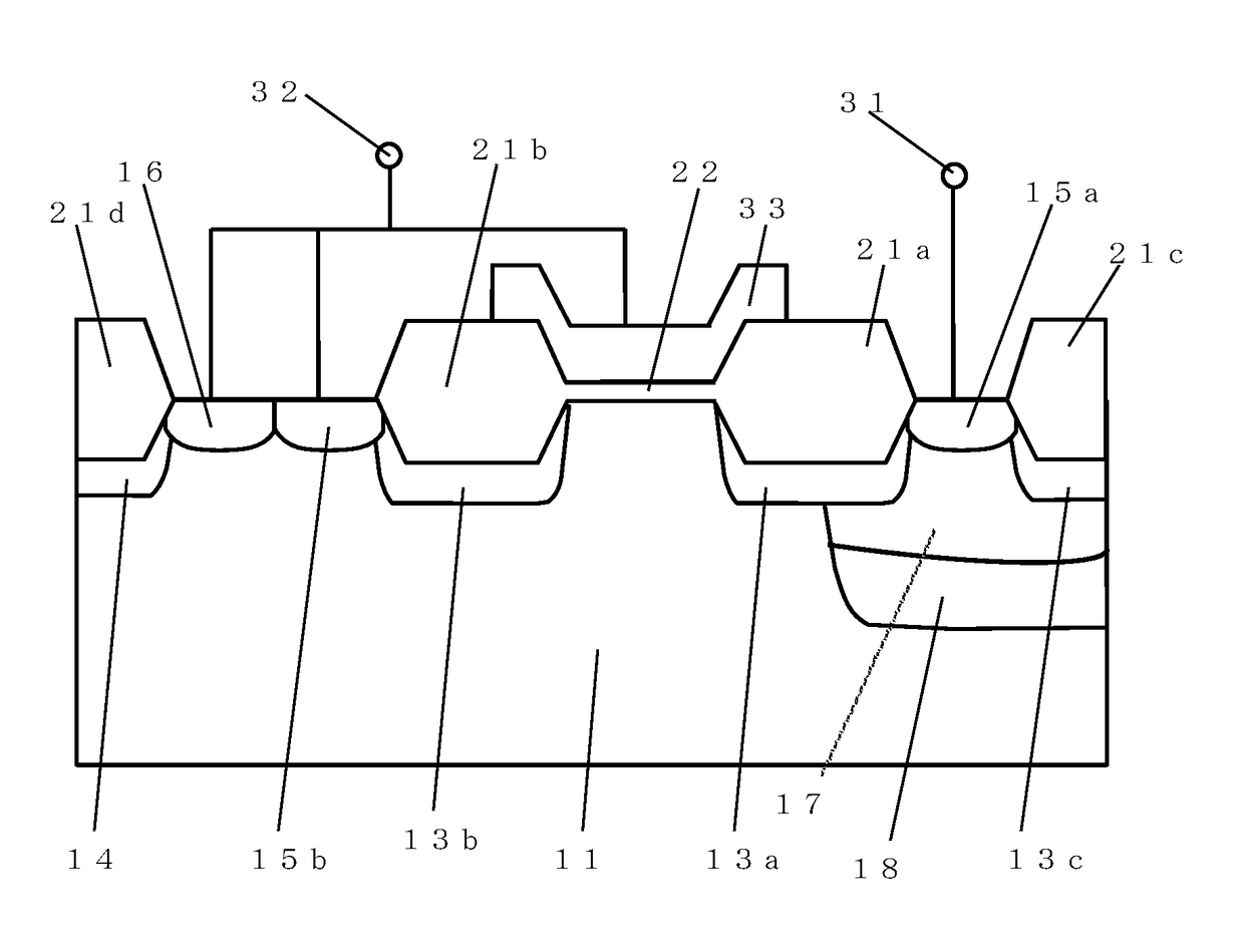
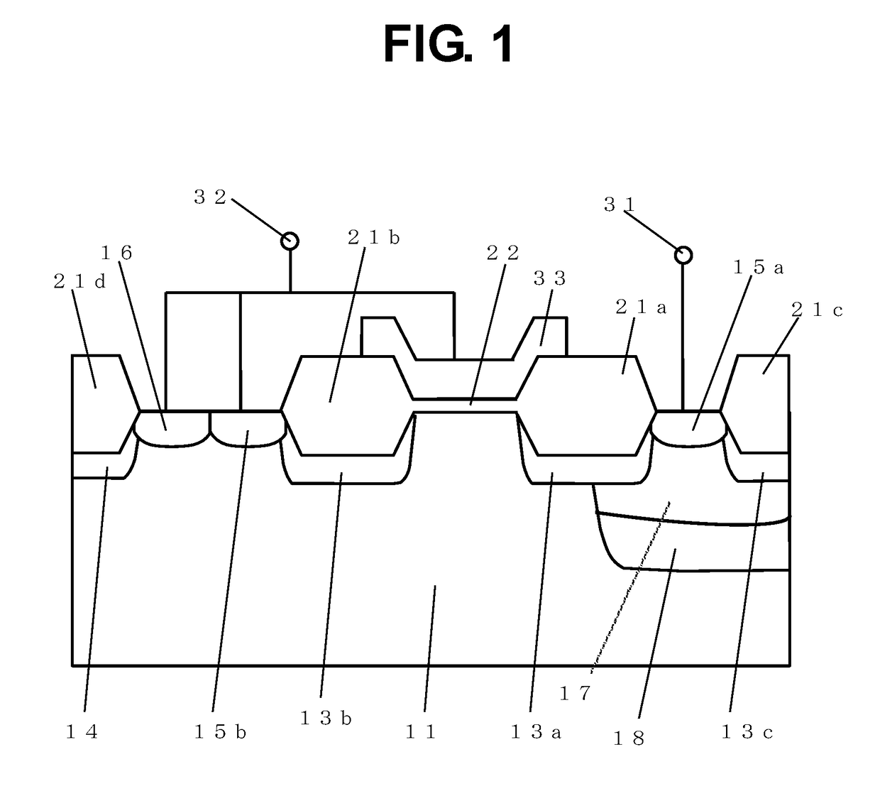
[0034]An embodiment of the present invention is described below with reference to the drawings. FIG. 1 is a view of a semiconductor device according to the present invention. As illustrated in FIG. 1, a gate insulating film 22 is formed on a P-type semiconductor substrate 11, and a gate electrode 33 is formed on the gate insulating film 22. LOCOS oxide films 21a and 21b are formed at the respective ends of the gate electrode 33. A first N-type low concentration diffusion layer 13a of a drain is formed under the LOCOS oxide film 21a and serves as an offset layer for easing the electric field concentration. An N-type high concentration diffusion layer 15a of the drain is formed so as to adjoin the first N-type low concentration diffusion layer 13a of the drain. The N-type high concentration diffusion layer 15a of the drain is connected to a drain electrode 31. A first N-type low concentration diffusion layer 13b of a source is an offset layer of the source and is formed under the LOCO...


PUM


Abstract

In an ESD protection element configured to protect a semiconductor device, a first N-type low concentration diffusion layer is formed, as an offset layer for easing electric field concentration, under a LOCOS oxide film formed at each end of the gate electrode, and a second N-type low concentration diffusion layer and a third low concentration diffusion layer are formed under an N-type high concentration diffusion layer on the drain side to set the point of breakdown at a level deep inside a substrate from a surface of the substrate. The hold voltage is thus raised to a voltage equal to or higher than the operating voltage and a noise can be relieved without increasing the element size of the ESD protection element even when the noise having a large amount of positive electric charge is applied to a Vdd supply terminal.

Description

RELATED APPLICATIONS[0001]This application claims priority under 35 U.S.C. §119 to Japanese Patent Application No. 2016-190175 filed on Sep. 28, 2016, the entire content of which is hereby incorporated by reference.BACKGROUND OF THE INVENTION1. Field of the Invention[0002]The present invention relates to an ESD protection element configured to prevent the breakdown of a semiconductor device having a high withstanding voltage from a surge and noise, typically, electrostatic discharge.2. Description of the Related Art[0003]A semiconductor device is provided with an electrostatic discharge (hereinafter abbreviated as ESD) protection element in order to protect internal elements from various surges and noises, typically, ESDs. Examples of the ESD protection element include diode elements, bipolar elements, and thyristor elements that are configured independently or parasitically. A diode, bipolar, or thyristor element as an ESD protection element in a semiconductor device is required to...

Claims


Application Information

Patent Timeline
IPC IPC(8): H01L29/06H01L29/10H01L29/66H01L29/78
CPCH01L29/0626H01L29/1045H01L29/66681H01L29/7816H01L23/60H01L29/78H01L29/42368H01L29/7834H01L29/7835H01L29/861H01L29/1087H01L27/0248H01L21/02576H01L21/02579H01L21/761
Inventor MINAMI, YUKIMASA
Owner ABLIC INC
Why Eureka
Try Eureka