Semiconductor device and electronic device

a semiconductor device and electronic device technology, applied in the direction of power consumption reduction, pulse technique, instruments, etc., can solve the problems of increasing the size of the n-channel transistor in the level shift circuit, increasing the area of the level shift circuit, increasing current, etc., to suppress the increase in the area of the semiconductor device, increasing the size of the transistor, and operating more stably

Inactive Publication Date: 2018-03-29
SEMICON ENERGY LAB CO LTD
View PDF2 Cites 4 Cited by
  • Summary
  • Abstract
  • Description
  • Claims
  • Application Information

AI Technical Summary

Benefits of technology

[0024]One embodiment of the present invention can provide a level shift circuit capable of operating more stably. One embodiment of the present invention can decrease the need for increasing the size of a transistor included in a level shift circuit. One embodiment of the present invention can s...

Problems solved by technology

However, the increase in size of the n-channel transistor in the level shift circuit is not desirable because problem...

Method used


Image

  • Semiconductor device and electronic device
  • Semiconductor device and electronic device
  • Semiconductor device and electronic device

Examples


embodiment 1

[0052]In this embodiment, a level shift circuit of one embodiment of the present invention will be described with reference to FIGS. 1 to 4, FIGS. 5A and 5B, and FIGS. 6A and 6B.

configuration example 1

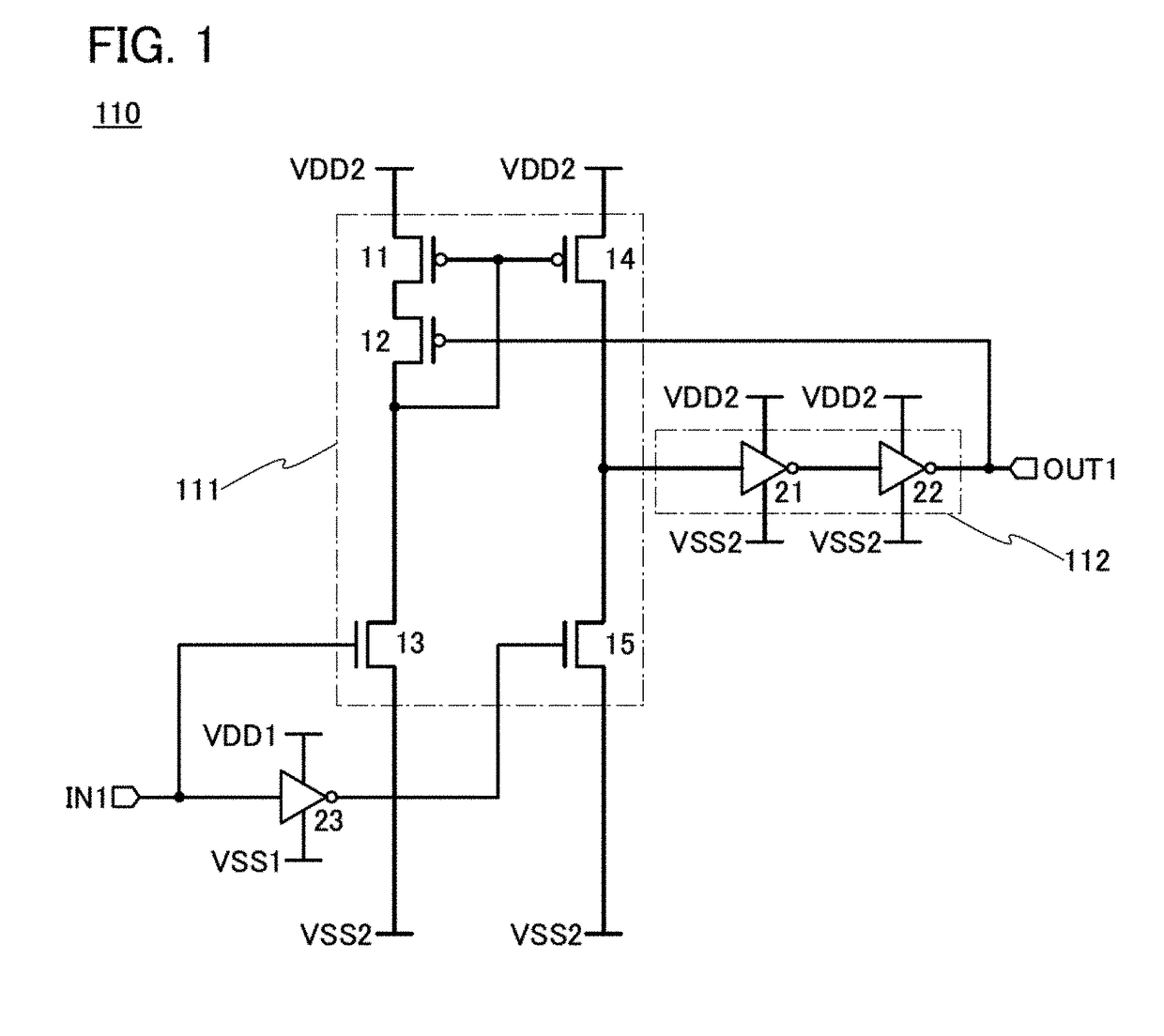
[0053]FIG. 1 illustrates a configuration example of a level shift circuit 110 in one embodiment of the present invention.

[0054]The level shift circuit 110 has a function of converting an input signal with an amplitude between a potential VDD1 and a potential VSS1 into an output signal with an amplitude between a potential VDD2 and a potential VSS2. In other words, the level shift circuit 110 has a function of converting an input signal into an output signal with a higher or lower amplitude voltage.

[0055]The potential VSS1 is preferably equal to the potential VSS2. Both the potential VSS1 and the potential VSS2 may be a ground potential.

[0056]The level shift circuit 110 includes a level shift unit 111 and a buffer circuit 112. Moreover, the level shift circuit 110 includes an input terminal IN1, an inverter circuit 23, and an output terminal OUT1.

[0057]The level shift unit 111 includes a transistor 11, a transistor 12, a transistor 13, a transistor 14, and a transistor 15. The transi...

configuration example 2

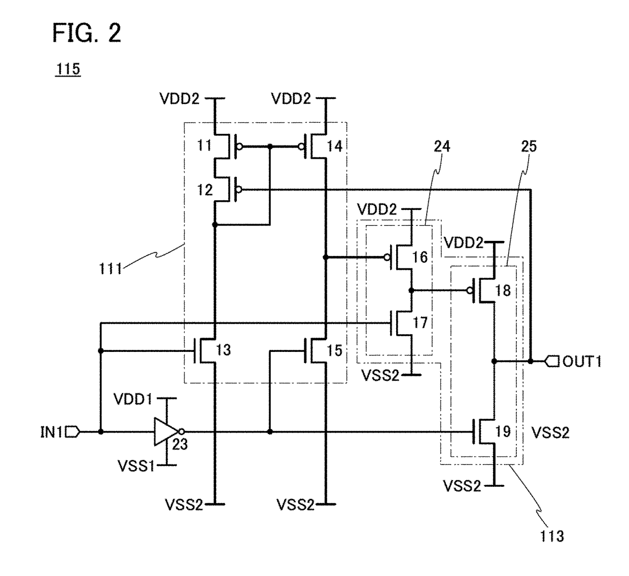
[0071]Next, a configuration of a level shift circuit 115 that has the same function as the level shift circuit 110 will be described with reference to FIG. 2.

[0072]The level shift circuit 115 differs from the level shift circuit 110 in including a buffer circuit 113 instead of the buffer circuit 112. That is, the level shift circuit 115 includes the level shift unit 111 and the buffer circuit 113. Moreover, the level shift circuit 115 includes the input terminal IN1, the inverter circuit 23, and the output terminal OUT1.

[0073]The buffer circuit 113 includes an inverter circuit 24 and an inverter circuit 25. Each of the inverter circuits 24 and 25 is an inverter circuit having two input terminals.

[0074]The inverter circuit 24 includes a transistor 16 and a transistor 17. One of a source and a drain of the transistor 16 is electrically connected to one of a source and a drain of the transistor 17.

[0075]The inverter circuit 25 includes a transistor 18 and a transistor 19. One of a sour...


PUM


Abstract

An object is to provide a level shift circuit that operates stably. A semiconductor device includes a level shift circuit including first to fourth transistors and a buffer circuit. One of a source and a drain (S/D) of the first transistor is connected to one of a source and a drain of the second transistor. The other of the source and the drain of the second transistor is connected to one of a source and a drain of the third transistor. A gate of the first transistor and a gate of the fourth transistor are connected to the other of the source and the drain of the second transistor and the one of the source and the drain of the third transistor. A gate of the third transistor is connected to a wiring to which an input signal is input. An input terminal of the buffer circuit is connected to one of a source and a drain of the fourth transistor. An output terminal of the buffer circuit is connected to a gate of the second transistor and a wiring to which an output signal is output.

Description

BACKGROUND OF THE INVENTION1. Field of the Invention[0001]One embodiment of the present invention relates to a semiconductor device and an electronic device.[0002]Note that one embodiment of the present invention is not limited to the above technical field. The technical field of the invention disclosed in this specification and the like relates to an object, a method, or a manufacturing method. Furthermore, one embodiment of the present invention relates to a process, a machine, manufacture, or a composition of matter. Specific examples of the technical field of one embodiment of the present invention disclosed in this specification include a semiconductor device, a display device, a light-emitting device, a power storage device, an imaging device, a memory device, a method for driving any of them, and a method for manufacturing any of them.2. Description of the Related Art[0003]High-resolution display devices are widely used. Integrated circuits (ICs) are used in source drivers of...

Claims


Application Information

Patent Timeline
IPC IPC(8): H03K3/356H03K3/012G11C11/412G09G3/36G09G3/20H03K19/00
CPCH03K3/356017H03K3/012H03K3/356139G11C11/412G09G3/3611G09G3/20H03K19/0013G11C19/28H03K19/018521G09G3/3233G09G2310/0289G09G2310/0291G09G3/3648G09G2330/021G09G2310/0297G09G2310/0286
Inventor YAMAMOTO, ROH
Owner SEMICON ENERGY LAB CO LTD
Why Eureka
Try Eureka