Semiconductor Memory Devices

a memory device and semiconductor technology, applied in the direction basic electric elements, electrical appliances, etc., can solve the problems of limited integrity of b>2/b>d semiconductor memory devices, high price of equipment used for micronization of patterns, etc., to improve improve the electrical characteristics of semiconductor memory devices, and reduce the cost

Active Publication Date: 2018-04-05
SAMSUNG ELECTRONICS CO LTD
View PDF4 Cites 41 Cited by
  • Summary
  • Abstract
  • Description
  • Claims
  • Application Information

AI Technical Summary

Benefits of technology

[0004]The present inventive concepts provide semiconductor memory devices having improved reliability.
[0009]According to example embodiments of the present inventive concepts, since semiconductor memory devices may include a vertical channel pattern having a small thickness, electron mobility of a channel can increase and electrical characteristics of the semiconductor memory devices can be improved.
[0010]Further, a lower semiconductor pattern may be inhibited or prevented from being excessively etched during a manufacturing process to reduce or prevent disconnection of the vertical channel pattern having the small thickness, which contacts the lower semiconductor pattern. As a result, semiconductor memory devices having improved reliability can be provided.

Problems solved by technology

However, since the equipment used for micronization of a pattern can be expensive, the integrity of the 2D semiconductor memory devices may be limited.

Method used


Image

  • Semiconductor Memory Devices
  • Semiconductor Memory Devices
  • Semiconductor Memory Devices

Examples


Embodiment Construction

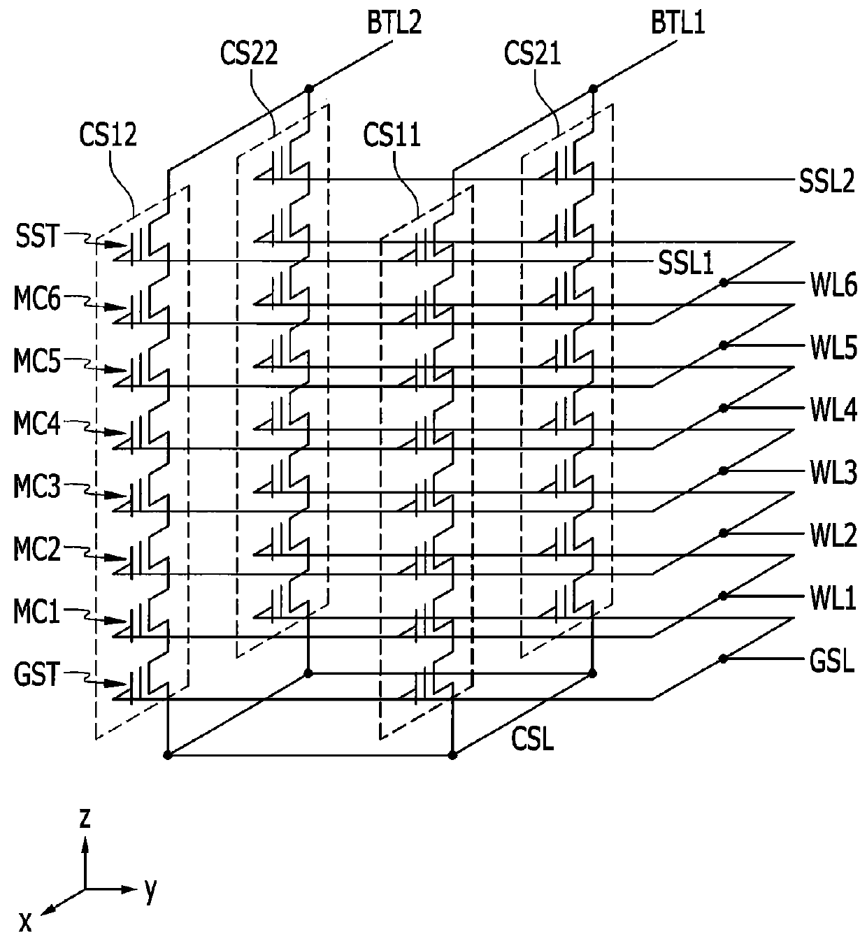
[0021]FIG. 1 is a schematic circuit diagram illustrating a 3D semiconductor memory cell array according to an example embodiment of the present inventive concepts.

[0022]Referring to FIG. 1, the memory cell array may include a plurality of cell strings CS11, CS12, CS21, and CS22 which extend in a vertical direction. The plurality of cell strings may have a vertical structure in which the plurality of cell strings extend in a perpendicular direction (e.g., a z direction) to a plane of a substrate upon which the plurality of cell strings are formed.

[0023]The plurality of cell strings CS11, CS12, CS21, and CS22 may include a ground selection transistor GST, a plurality of memory cell transistors MC1, MC2, . . . , MC6, and a string selection transistor SST which are connected in series, respectively. In FIG. 1, it is illustrated that each of the cell strings CS11, CS12, CS21, and CS22 has one string selection transistor SST, but the present inventive concepts are not limited thereto. Fur...


PUM


Abstract

A semiconductor memory device may include: a stacking structure including a plurality of insulating layers and a plurality of gate electrodes alternately stacked on a substrate; a lower semiconductor pattern that protrudes from the top of the substrate; a vertical insulating pattern that extends in a vertical direction from the substrate and penetrates the stacking structure; and a vertical channel pattern on the inner surface of the vertical insulating pattern and contacting the lower semiconductor pattern, wherein an upper part of the lower semiconductor pattern includes a recess region including a curve-shaped profile, and in the recess region, the outer surface of a lower part of the vertical channel pattern contacts the lower semiconductor pattern along a curve of the recess region.

Description

CROSS-REFERENCE TO RELATED APPLICATION[0001]This application claims the benefit of priority under 35 U.S.C. § 119 to Korean Patent Application No. 10-2016-0128216 filed in the Korean Intellectual Property Office on Oct. 5, 2016, the entire contents of which are incorporated herein by reference.BACKGROUND(a) Field[0002]The present inventive concepts relate to semiconductor memory devices.(b) Description of the Related Art[0003]The price and performance demands of consumers have created an increasing need for semiconductor memory devices with improved integrity. In the case of 2D or planar semiconductor memory devices, since the integrity can be determined, in part, by an area occupied by a unit memory cell, the integrity may be influenced by a level of a micro pattern forming technology. However, since the equipment used for micronization of a pattern can be expensive, the integrity of the 2D semiconductor memory devices may be limited.SUMMARY[0004]The present inventive concepts prov...

Claims


Application Information

Patent Timeline
Patent Type & Authority Applications(United States)
IPC IPC(8): H01L27/11556H01L29/08H01L27/11582H01L29/10
CPCH01L27/11556H01L29/0847H01L27/11582H01L29/42364H01L29/42324H01L29/4234H01L29/1037H10B43/10H10B43/35H10B43/20H10B43/27H10B41/10H10B41/41H10B41/27H10B43/30H10B41/30
Inventor KIM, SUNG GILCHOI, JI-HOONKIM, DONGKYUMNOH, JINTAEKIM, SEULYEKIM, HONG SUKNAM, PHIL OUKAHN, JAEYOUNG
Owner SAMSUNG ELECTRONICS CO LTD
Why Eureka
Try Eureka