Methods for Fabricating Semiconductor Devices Including Surface Treatment Processes

a technology of surface treatment and semiconductor devices, applied in semiconductor/solid-state device manufacturing, basic electric elements, electric devices, etc., can solve problems such as surface damag

Active Publication Date: 2018-04-12
SAMSUNG ELECTRONICS CO LTD
View PDF3 Cites 6 Cited by
  • Summary
  • Abstract
  • Description
  • Claims
  • Application Information

AI Technical Summary

Benefits of technology

[0005]Some embodiments of the inventive concepts may provide methods for fabricating semiconductor devices that may provide enhanced performance and reliability by recovering a quality of a low-k insulating film that is damaged by a plasma process.
[0006]Some embodiments of the inventive concepts may provide semiconductor devices that may provide enhanced performance and reliability of the device by recovering a quality of a low-k insulating, film that is damaged by a plasma process.
[0009]According to some embodiments of the inventive concepts, methods for fabricating a semiconductor device may be provided. A method for fabricating a semiconductor device may include forming an insulating film on a substrate and forming a metal wiring region in the insulating film. The method may include exposing a surface of the insulating film and a surface of the metal wiring region to a plasma in a first surface treatment process, then exposing the surface of the insulating film to a recovery gas in a second surface treatment, and then forming an etch stop layer on the metal wiring region and the insulating film. The recovery gas may increase a carbon concentration of the surface of the insulating film.

Problems solved by technology

The first surface treatment may treat a surface of the metal wiring region and may damage a surface of the first interlayer insulating firm.

Method used


Image

  • Methods for Fabricating Semiconductor Devices Including Surface Treatment Processes
  • Methods for Fabricating Semiconductor Devices Including Surface Treatment Processes
  • Methods for Fabricating Semiconductor Devices Including Surface Treatment Processes

Examples


Embodiment Construction

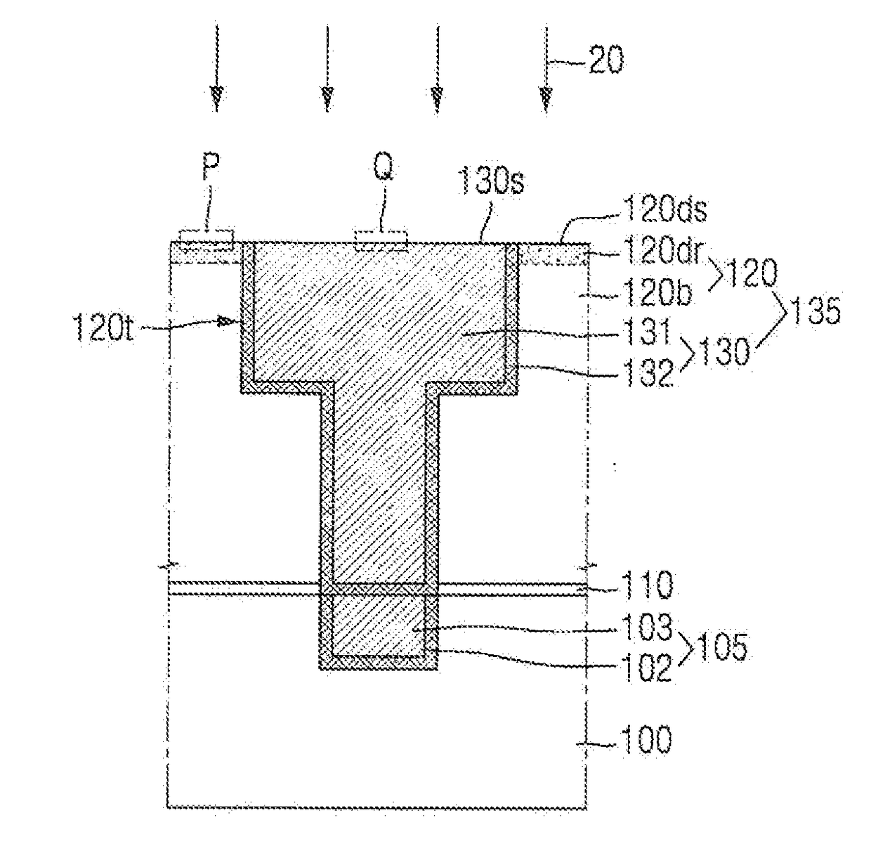
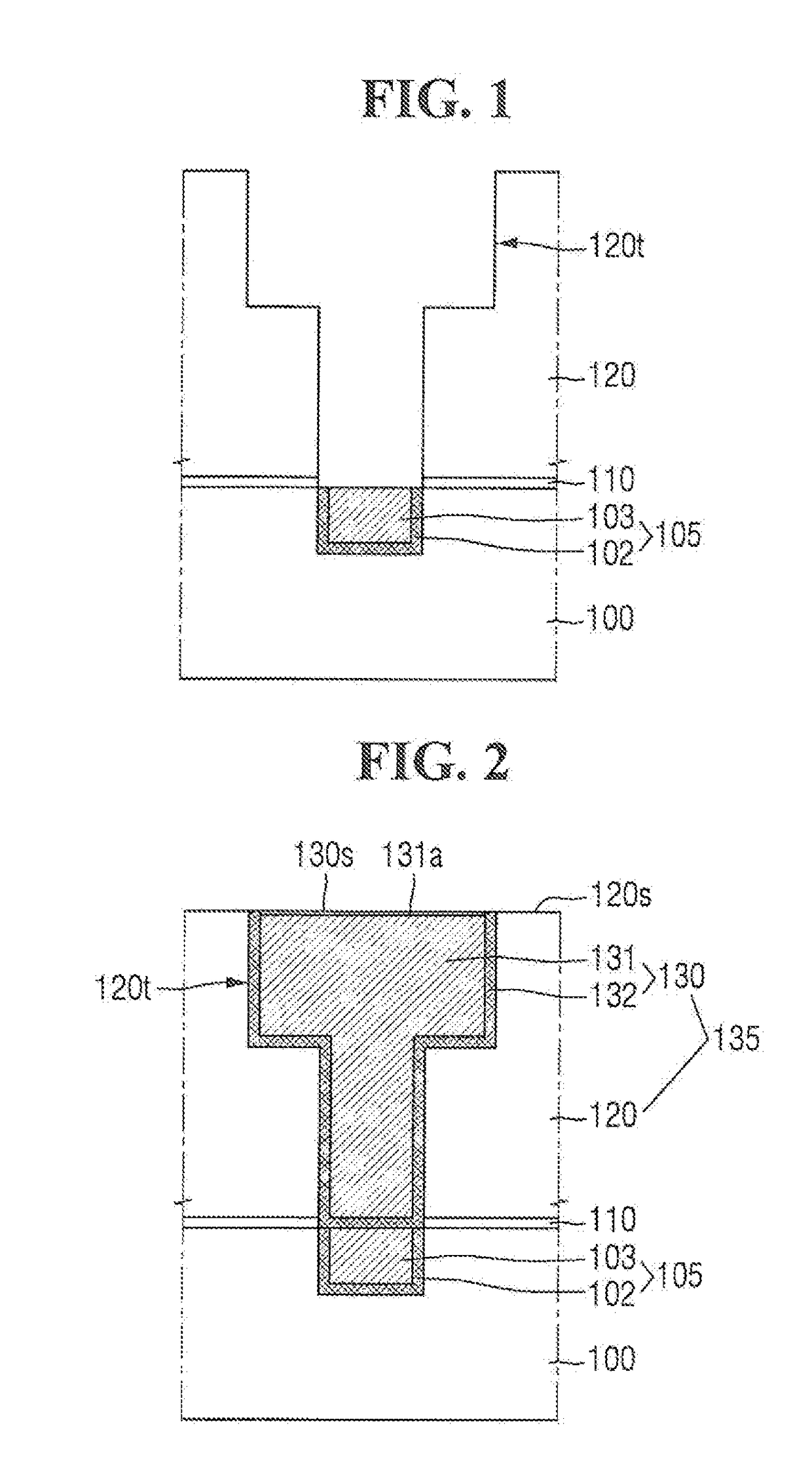
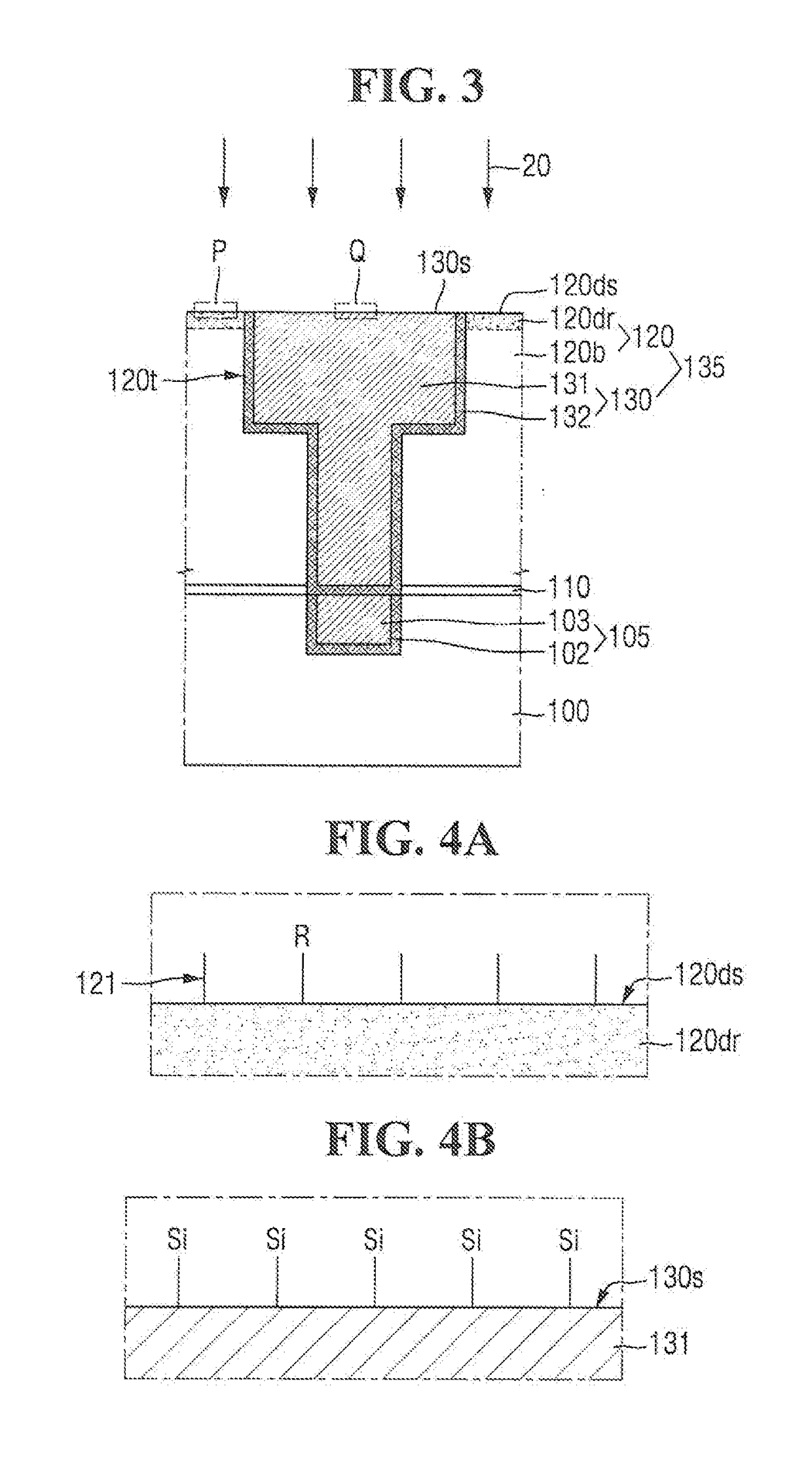
[0022]The inventive concepts will now be described more fully hereinafter with reference to the accompanying drawings, in which exemplary embodiments of the inventive concepts are shown. The inventive concepts and methods of achieving them will be apparent from the following exemplary embodiments that will be described in more detail with reference to the accompanying drawings. The embodiments of the inventive concepts may, however, be embodied in different forms and should not be constructed as limited to the embodiments set forth herein, Rather, these embodiments are provided so that this disclosure will be thorough and complete, and will fully convey the scope of the inventive concepts to those skilled in the art.

[0023]The drawings are intended to illustrate the general characteristics of methods, structures and / or materials utilized in certain some embodiments and to supplement the written description provided below. These drawings may not, however, to scale and may not precisel...


PUM

PropertyMeasurementUnit
conductiveaaaaaaaaaa
insulatingaaaaaaaaaa
concentrationaaaaaaaaaa

Abstract

Methods for fabricating semiconductor devices may provide enhanced performance and reliability by recovering quality of a low-k insulating film damaged by a plasma process. A method may include forming a first interlayer insulating film having a trench therein on a substrate, filling at least a portion of the trench with a metal wiring region, exposing a surface of the metal wiring region and a surface of the first interlayer insulating film to a plasma in a first surface treatment process, then exposing the surface of the first interlayer insulating film to a recovery gas containing a methyl group (—CH3) in a second surface treatment process, and then forming an etch stop layer on the metal wiring region and the first interlayer insulating film.

Description

REFERENCE TO PRIORITY APPLICATION[0001]This application claims priority under 35 U.S.C. § 119 to Korean Patent Application No. 10-2016-0131088, filed Oct. 11, 2016 in the Korean Intellectual Property Office, the contents of which are hereby incorporated herein by reference in their entirety.BACKGROUND1. Technical field[0002]Embodiments of the inventive concepts relate to methods for fabricating semiconductor devices, and more specifically, to methods for fabricating semiconductor devices using a low-k material as an interlayer insulating film.2. Description of the Related Art[0003]In fabrication of semiconductor devices, dielectric constant k of a dielectric film may decrease as the semiconductor devices are continuously scaled. Minimizing integration damage for low-k dielectric films may therefore be useful when decreasing a feature size.[0004]Accordingly, it may be useful to improve resistive capacitance and reliability of the dielectric film when decreasing the feature size.SUMMA...

Claims


Application Information

Patent Timeline
Patent Type & Authority Applications(United States)
IPC IPC(8): H01L21/768
CPCH01L21/76877H01L21/76814H01L21/76883H01L21/7682H01L21/76829H01L21/76832H01L21/76834H01L21/76849H01L21/76856H01L21/76826H01L21/02252H01L21/76838H01L21/02274H01L21/02172H01L21/76888
Inventor NGUYEN, VIET HALEE, NAE INOSZINDA, THOMASKIM, BYUNG HEEBAEK, JONG MINYIM, TAE JIN
Owner SAMSUNG ELECTRONICS CO LTD
Why Eureka
Try Eureka