Amoled pixel driving circuit and pixel driving method

a driving circuit and pixel technology, applied in the field of display technology, can solve the problems of increasing the complexity of data signals, inability to meet the brightness requirement of panels, and inconsistent current passing through organic light emitting diodes

Active Publication Date: 2018-04-12
SHENZHEN CHINA STAR OPTOELECTRONICS TECH CO LTD
View PDF0 Cites 17 Cited by
  • Summary
  • Abstract
  • Description
  • Claims
  • Application Information

AI Technical Summary

Benefits of technology

[0061]The benefits of the present invention are: the present invention provides an AMOLED pixel driving circuit and a pixel driving method. By utilizing the dual gate thin film transistor to be the drive thin film transistor, in the pre-charge stage, the second, the third scan drive signals are employed to control the third, the fourth and the fifth thin film transistors to be activated to write the preset voltage to the bottom gate of the first thin film transistor, i.e. the drive thin film transistor, and to write the power source voltage to the top gate; in the threshold voltage programming stage, the third scan drive signal is employed to control the fourth thin film transistor to be deactivated to drop the voltage of the top gate of the first thin film transistor, and the threshold voltage is raised until the threshold voltage is lifted up to Vth=Vpre−VOLED; in the driv

Problems solved by technology

Meanwhile, the threshold voltage drift also will happen after the organic light emitting diode is used in a long time, which leads to that the current passing through the organic light emitting diode is not consistent with the desired current, and the panel brightness cannot satisfy the requirement.
However, after the single gate thin film transistor suffers the stresses of the voltage and the light irradiation, the threshold voltage commonly drifts forward and increases, and thus the data signal has

Method used


Image

  • Amoled pixel driving circuit and pixel driving method
  • Amoled pixel driving circuit and pixel driving method
  • Amoled pixel driving circuit and pixel driving method

Examples


Embodiment Construction

[0071]For better explaining the technical solution and the effect of the present invention, the present invention will be further described in detail with the accompanying drawings and the specific embodiments.

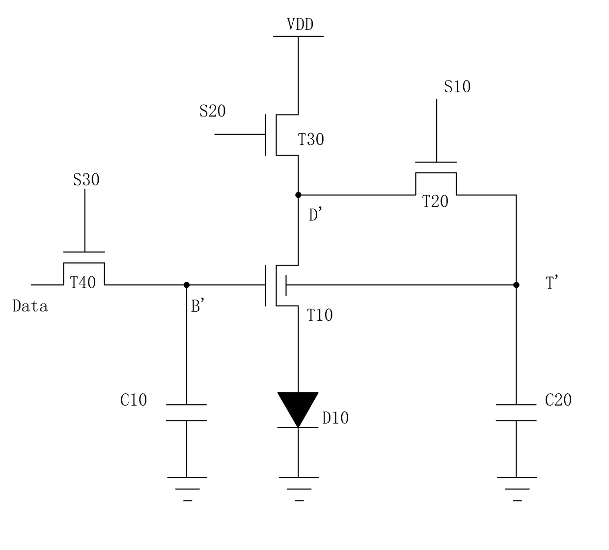
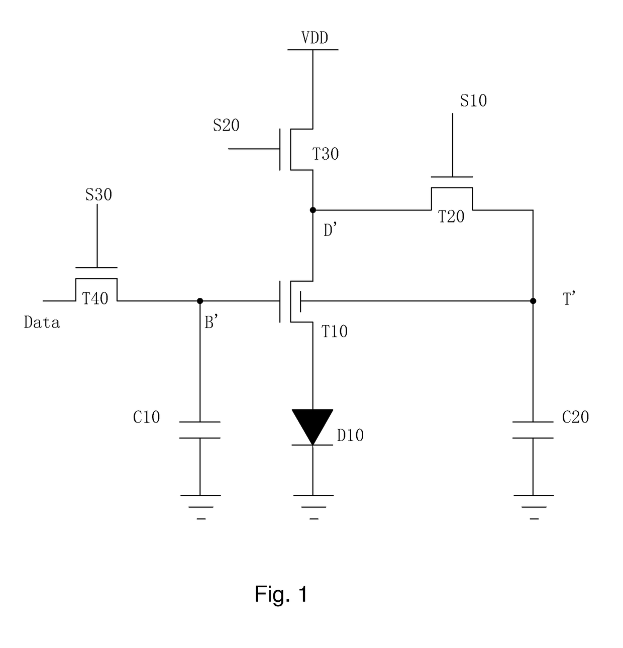
[0072]Please refer to FIG. 3 and FIG. 4, together. The present invention first provides an AMOLED pixel driving circuit, and the AMOLED pixel driving circuit utilizes a 5T2C structure, and comprises: a first thin film transistor T1, a second thin film transistor T2, a third thin film transistor T3, a fourth thin film transistor T4, a fifth thin film transistor T5, a first capacitor C1, a second capacitor C2 and an organic light emitting diode D1, wherein the first thin film transistor is employed to be a drive thin film transistor, and the second thin film transistor T1 is employed to be a switch thin film transistor T2.

[0073]Significantly, the first thin film transistor T1 is a dual gate thin film transistor, in which the stress influence of the voltage and light irradiation ...


PUM


Abstract

The present invention provides an AMOLED pixel driving circuit and a pixel driving method. By utilizing the dual gate thin film transistor to be the drive thin film transistor, in the pre-charge stage, the preset voltage (Vpre) is written to the bottom gate (BG) of the first thin film transistor (T1), and the power source voltage (VDD) is written to the top gate; in the threshold voltage programming stage, the voltage of the top gate (TG) of the first thin film transistor (T1) drops, and the threshold voltage is raised until the threshold voltage is lifted up to Vth=Vpre−VOLED; in the drive stage, the voltage of the top gate (TG) is kept unchanged to keep the threshold voltage remaining to be Vth=Vpre−VOLED, and the data signal Data drives the first thin film transistor (T1) to be activated to make the organic light emitting diode (D1) emit light.

Description

FIELD OF THE INVENTION[0001]The present invention relates to a display technology field, and more particularly to an AMOLED pixel driving circuit and a pixel driving method.BACKGROUND OF THE INVENTION[0002]The Organic Light Emitting Display (OLED) possesses many outstanding properties of self-illumination, low driving voltage, high luminescence efficiency, short response time, high clarity and contrast, near 180° view angle, wide range of working temperature, applicability of flexible display and large scale full color display. The OLED is considered as the most potential display device. The OLED can be categorized into two major types according to the driving methods, which are the Passive Matrix OLED (PMOLED) and the Active Matrix OLED (AMOLED), i.e. two types of the direct addressing and the Thin Film Transistor (TFT) matrix addressing. The AMOLED comprises pixels arranged in array and belongs to active display type, which has high lighting efficiency and is generally utilized fo...

Claims


Application Information

Patent Timeline
IPC IPC(8): H01L27/32G09G3/3258G09G3/3266
CPCH01L27/3248H01L27/3262G09G3/3258H01L27/3265G09G3/3266G09G3/3233G09G2320/0233G09G2300/0819G09G2300/0842G09G2320/045H10K59/123H10K59/1213H10K59/1216
Inventor NIE, CHENGLEI
Owner SHENZHEN CHINA STAR OPTOELECTRONICS TECH CO LTD
Why Eureka
Try Eureka