Manufacturing method for wiring board

a manufacturing method and wiring board technology, applied in the direction of manufacturing tools, lapping machines, semiconductor/solid-state device details, etc., can solve the problems of failure to form the wiring board flat, failure to form the circuit pattern in accordance with its design, and the factor of a malfunction, so as to suppress the effect of roughness

Active Publication Date: 2018-04-12
DISCO CORP
View PDF5 Cites 3 Cited by
  • Summary
  • Abstract
  • Description
  • Claims
  • Application Information

AI Technical Summary

Benefits of technology

[0005]Therefore, it is an object of the present invention to suppress occurrence of roughness on a circuit pattern of a wiring board thereby to allow the circuit pattern to be formed in accordance with its design.
[0010]The manufacturing methods for a wiring board according to the present invention exhibit an advantageous effect that roughness can be suppressed from occurring on a circuit pattern of a wiring board and the circuit pattern can be formed in accordance with a design therefor.

Problems solved by technology

Therefore, if the wiring board is warped or is not flat, then it is difficult to favorably connect electrodes of semiconductor chips or various electric parts to be mounted and electrodes of the wiring boards to each other, which makes a factor of a malfunction.
Although the printed wiring board disclosed in Japanese Patent Laid-Open No. 2013-80823 suppresses occurrence of warpage when a thermal history is applied to the printed wiring board as described above, only such suppression of deformation by a thermal history results in failure to form the wiring board flat when the core substrate originally has a warped shape or is not flat.
However, depending upon a component of material contained in the insulating layer, there is the possibility that the machining of both the insulating layer and metal that forms the circuit pattern may give rise to roughness (smear) on the exposed face (machined face) of the circuit pattern, resulting in failure to form the circuit pattern in accordance with its design.

Method used


Image

  • Manufacturing method for wiring board
  • Manufacturing method for wiring board
  • Manufacturing method for wiring board

Examples


first embodiment

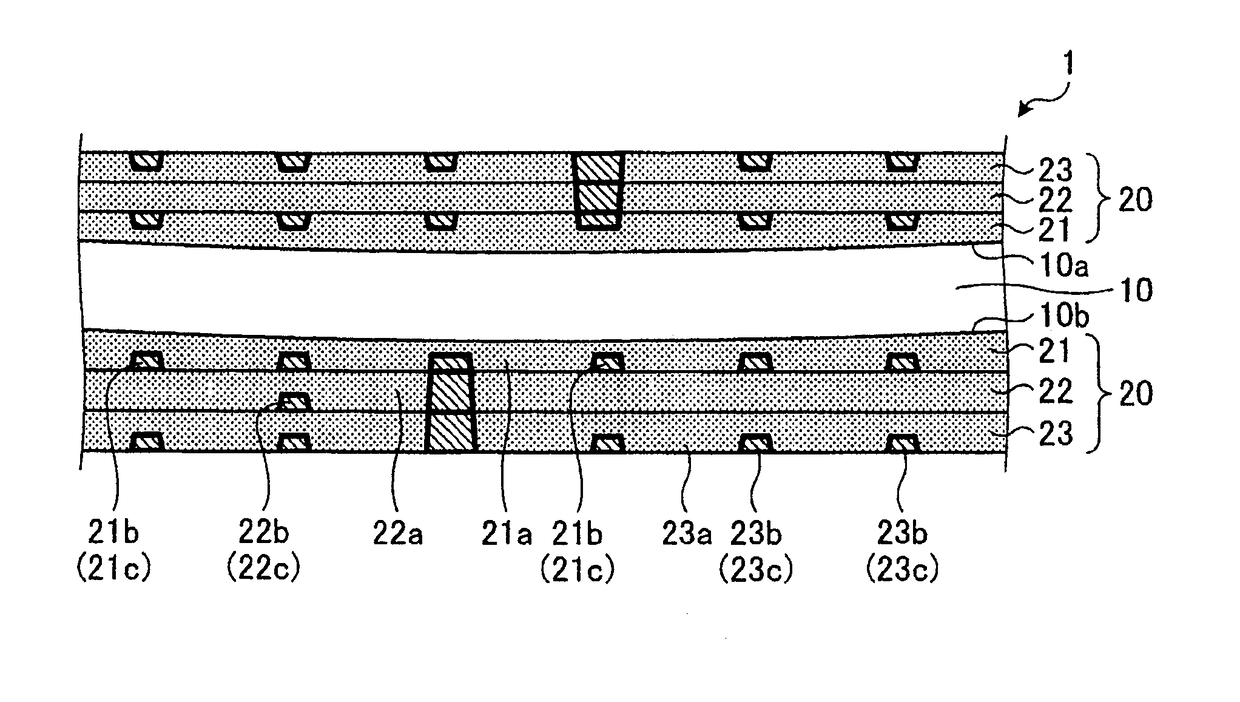
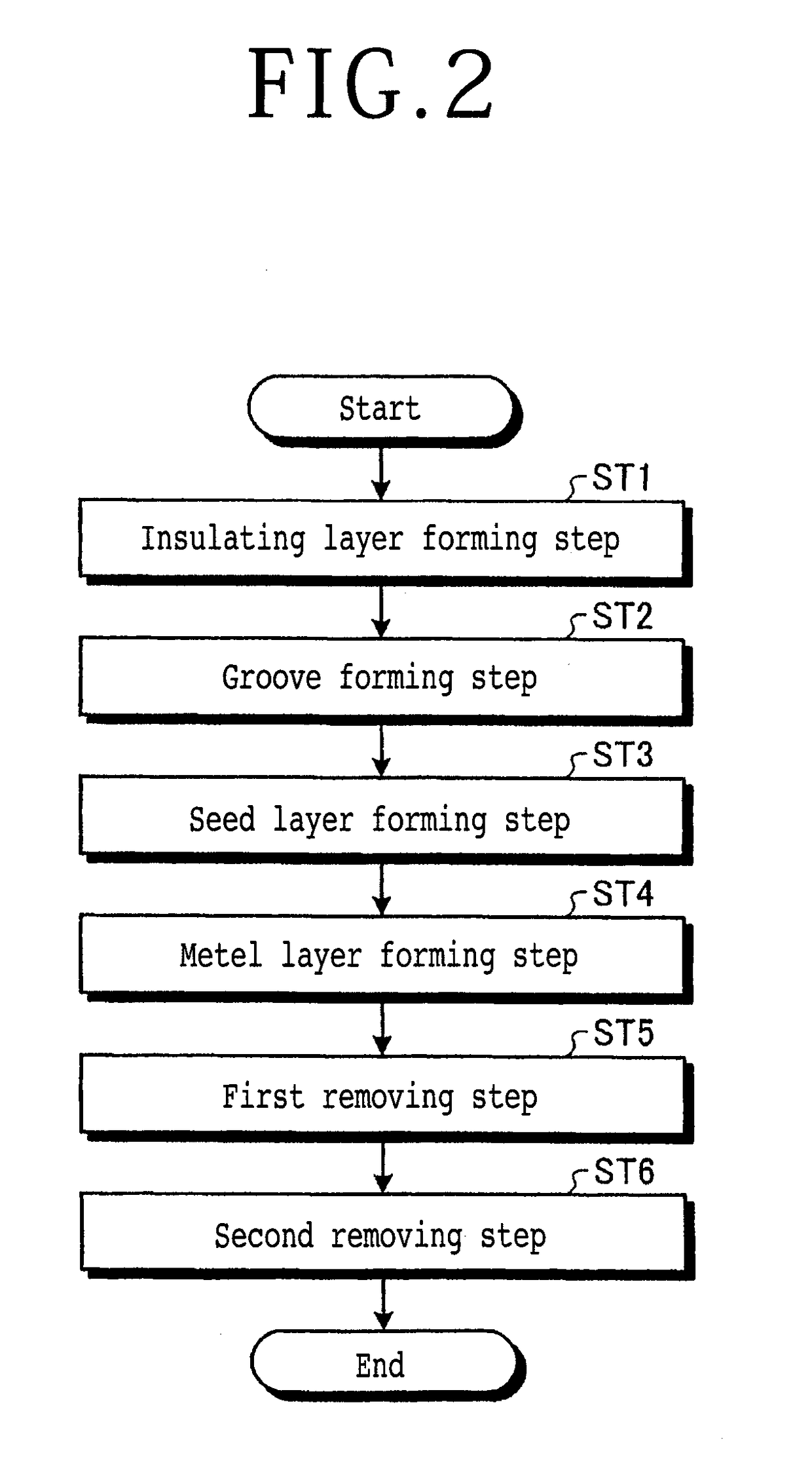
[0028]A manufacturing method for a wiring board according to a first embodiment of the present invention is described with reference to the accompanying drawings. FIG. 1 is a cross sectional view depicting a wiring board manufactured by the manufacturing method for a wiring board according to the first embodiment. The wiring board 1 depicted in FIG. 1 includes a rewiring layer. The wiring board 1 is an interposer, a printed wiring board or the like in which semiconductor chips or various electric parts are mounted and incorporated and continuity between their electrodes and other parts is secured. In the present embodiment, the wiring board 1 is an interposer that has semiconductor chips mounted thereon and is connected to a printed wiring board such that electrodes of the semiconductor chips and a wiring pattern of the printed wiring board are connected to each other in accordance with a predetermined pattern. As illustrated in FIG. 1, the wiring board 1 includes a core substrate 1...

second embodiment

[0052]Subsequently, a manufacturing method for a wiring board according to a second embodiment of the present invention is described. The manufacturing method for a wiring board according to the second embodiment is similar to the manufacturing method for a wiring board according to the first embodiment except that it is different in techniques in the first removing step ST5 and the second removing step ST6 illustrated in FIG. 2. In the following, the first removing step ST5 and the second removing step ST6 in the second embodiment are described with reference to the drawings, and description of the steps other than the first removing step ST5 and the second removing step ST6 is omitted herein. FIG. 11 is a schematic view illustrating a manner in which the first removing step ST5 in the manufacturing method for a wiring board according to the second embodiment is carried out, and FIG. 12 is a schematic view illustrating a manner in which the second removing step ST6 in the manufactu...


PUM

PropertyMeasurementUnit
thicknessaaaaaaaaaa
thicknessaaaaaaaaaa
heightaaaaaaaaaa

Abstract

A method for manufacturing a wiring board that has a rewiring layer on a surface thereof includes forming an insulating layer on a core substrate, forming a groove, in which a wiring layer of a circuit pattern is to be provided, on the insulating layer, forming a metal seed layer on an exposed face of the insulating layer on which the groove is formed, electrodepositing metal, which is to form the wiring layer, by plating to fill the groove with the metal to form a metal layer on the seed layer, machining the metal layer by a cutting tool to remove the metal layer up to a position not reaching the top of the insulating layer, and performing etching or a CMP process to expose the top of the insulating layer thereby to form the wiring layer in the groove and flatten an exposed face of the wiring layer.

Description

BACKGROUND OF THE INVENTIONField of the Invention[0001]The present invention relates to a manufacturing method for a wiring board.Description of the Related Art[0002]Conventionally, a technology is known which relates to a wiring board such as an interposer or a printed wiring board in which semiconductor chips or various electric parts are mounted and incorporated such that continuity between electrodes of them and other parts is secured. The wiring board has a rewiring layer. For example, in Japanese Patent Laid-Open No. 2001-196743, a printed wiring board of the build-up type is disclosed in which conductor layers and organic insulating layers are alternately stacked on front and rear faces of a core substrate.[0003]Japanese Patent Laid-Open No. 2013-80823 discloses a printed wiring board that is manufactured by providing a first insulating layer, which includes a reinforcing material impregnated with resin, on each of the opposite faces of a core substrate containing reinforcing...

Claims


Application Information

Patent Timeline
Patent Type & Authority Applications(United States)
IPC IPC(8): H05K3/26H01L23/498H01L23/00H01L21/48H05K3/00H05K3/10C25D7/12C25D5/48B24B37/04
CPCH05K3/26H01L23/49822H01L23/49838H01L23/562H01L21/4857H05K3/0044H05K3/107C25D7/123C25D5/48B24B37/042H05K3/043H05K2203/025H05K2203/0228H05K3/045H05K3/465H05K2203/0346H05K3/04Y10T29/49155
Inventor CHEN, YEWEI, FRANK
Owner DISCO CORP
Why Eureka
Try Eureka