Thin Film Transistor Substrate Having Color Filter

Active Publication Date: 2018-05-03
LG DISPLAY CO LTD
View PDF1 Cites 0 Cited by
  • Summary
  • Abstract
  • Description
  • Claims
  • Application Information

AI Technical Summary

Benefits of technology

[0029]The thin film transistor substrate for the liquid crystal display according to the present disclosure comprises a thin film transistor and a color filter on the same substrate. Therefore, the alignment margin for joining two substrates is not considered so that the high aperture ratio is ensured. Especially, the present disclosure suggests a best structure which is proper to get high aperture

Problems solved by technology

However, the horizontal electric field type LCD may have demerits such as low aperture ratio and transitivity ratio of the back light.
Even though the COT structure has some merits, the manufacturing proc

Method used


Image

  • Thin Film Transistor Substrate Having Color Filter
  • Thin Film Transistor Substrate Having Color Filter
  • Thin Film Transistor Substrate Having Color Filter

Examples


first embodiment

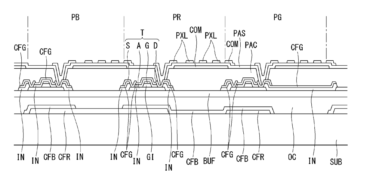
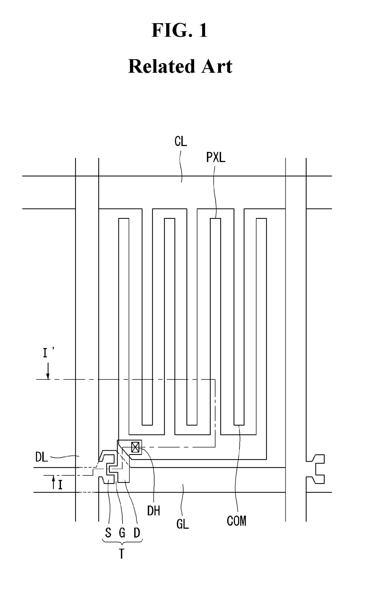
[0040]Referring to FIGS. 4 to 8, we will explain about the first embodiment of the present disclosure. FIG. 4 is a plan view illustrating a structure of a liquid crystal display according to the first embodiment of the present disclosure. FIG. 5 is a cross sectional view illustrating a structure of a liquid crystal display by cutting along the line I-I′ according to the first embodiment of the present disclosure. FIGS. 6 to 8 are plan views illustrating the patterns of the color filters according to the first embodiment of the present disclosure.

[0041]Referring to FIGS. 4 and 5, the liquid crystal display according to the first embodiment of the present disclosure comprises a gate line GL running to a first (i.e., horizontal) direction and a data line DL running to a second (i.e., vertical) direction on a substrate SUB. As a plurality of the gate lines GL is crossing with a plurality of the data lines DL, a plurality of pixel areas PA are defined as arraying in a matrix manner. At e...

second embodiment

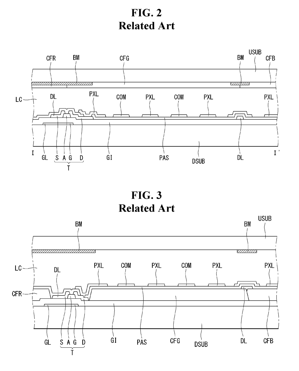
[0056]Hereinafter, referring to FIG. 9, we will explain about the second embodiment of the present disclosure. In the first embodiment, we explained about the structure of the liquid crystal display in which the green color filter is used for the intermediate insulating layer. In the second embodiment, we will explain about the structure of the liquid crystal display in which an extra intermediate insulating layer is included. FIG. 9 is a cross sectional view illustrating a structure of a liquid crystal display according to the second embodiment of the present disclosure.

[0057]The structure of the liquid crystal display according to the second embodiment of the present disclosure is very similar with that of the first embodiment. The difference is on that an additional intermediate insulating layer is included under the green color filter.

[0058]Referring to FIG. 9, a red color filter CFR is firstly deposited on a substrate SUB. The red color filter CFR has the same pattern with that...


PUM


Abstract

The present disclosure relates to a thin film transistor substrate having a color filter layer. The present disclosure provides a thin film transistor substrate comprising: a plurality of pixel areas disposed in a matrix manner on a substrate, each pixel area including an aperture area and a non-aperture area; a first color filter and a second color filter stacked at the non-aperture area on the substrate; an overcoat layer disposed on the first color filter and the second color filter; a semiconductor layer disposed at the non-aperture area on the overcoat layer; a gate insulating layer and a gate electrode stacked on a middle portion of the semiconductor layer; a third color filter at the non-aperture area on the semiconductor layer and the gate electrode; and a source electrode and a drain electrode disposed on the third color filter.

Description

CROSS-REFERENCE TO RELATED APPLICATION[0001]This application claims priority to Republic of Korea Patent Application No. 10-2016-0144000 filed on Oct. 31, 2016, which is incorporated by reference herein in its entirety.BACKGROUNDTechnical Field[0002]The present disclosure relates to a thin film transistor substrate having a color filter layer. Especially, the present disclosure relates to a thin film transistor substrate in which color filter layers are formed with the thin film transistor and any one color filter layer is used for the intermediate insulating layer of the thin film transistor.Discussion of the Related Art[0003]The liquid crystal display device represents video data by controlling the light transitivity of the liquid crystal layer using the electric fields. According to the direction of the electric field, the LCD can be classified in the two major types; one is vertical electric field type and the other is the horizontal electric field type.[0004]For the vertical el...

Claims


Application Information

Patent Timeline
IPC IPC(8): G02F1/1368H01L27/12G02F1/1343G02F1/1333G02F1/1362
CPCG02F1/1368H01L27/124G02F1/134309G02F1/133345G02F1/136227G02F1/136286G02F1/13439G02F2001/136222G02F2201/121G02F2201/123G02F1/1333G02F1/134363G02F1/1362G02F1/133357G02F1/136222G02F1/136209G02F1/136231G02F1/13685H01L29/78618H01L29/78606G02F2201/48G02F2201/40
Inventor WOO, CHANGSEUNGLEE, BYUNGHYUNHONG, SOONHWANWON, GYUSIK
Owner LG DISPLAY CO LTD
Why Eureka
Try Eureka