Semiconductor memory device

a memory device and semiconductor technology, applied in the field can solve problems such as failure of operation of semiconductor memory devices, and achieve the effect of improving operational reliability

Active Publication Date: 2018-05-10
SK HYNIX INC
View PDF2 Cites 74 Cited by
  • Summary
  • Abstract
  • Description
  • Claims
  • Application Information

AI Technical Summary

Benefits of technology

[0007]Various embodiments are directed to a semiconduct

Problems solved by technology

However, when a three-dimensional semiconductor memory device having a vertical stacked structure is manufactured, a misalignment may occur between

Method used


Image

  • Semiconductor memory device
  • Semiconductor memory device
  • Semiconductor memory device

Examples


Embodiment Construction

[0030]Hereinafter, various exemplary embodiments will be described in detail with reference to the accompanying drawings. In the drawings, the thicknesses and the intervals of elements are exaggerated for convenience of illustration, and may be exaggerated compared to an actual physical thickness. In describing the present invention, well-known features which are peripheral to the principal point of the present invention may be omitted. It should also be noted that in giving reference numerals to elements of each drawing, like reference numerals may refer to like elements shown in different drawings.

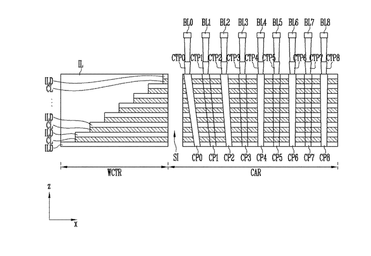
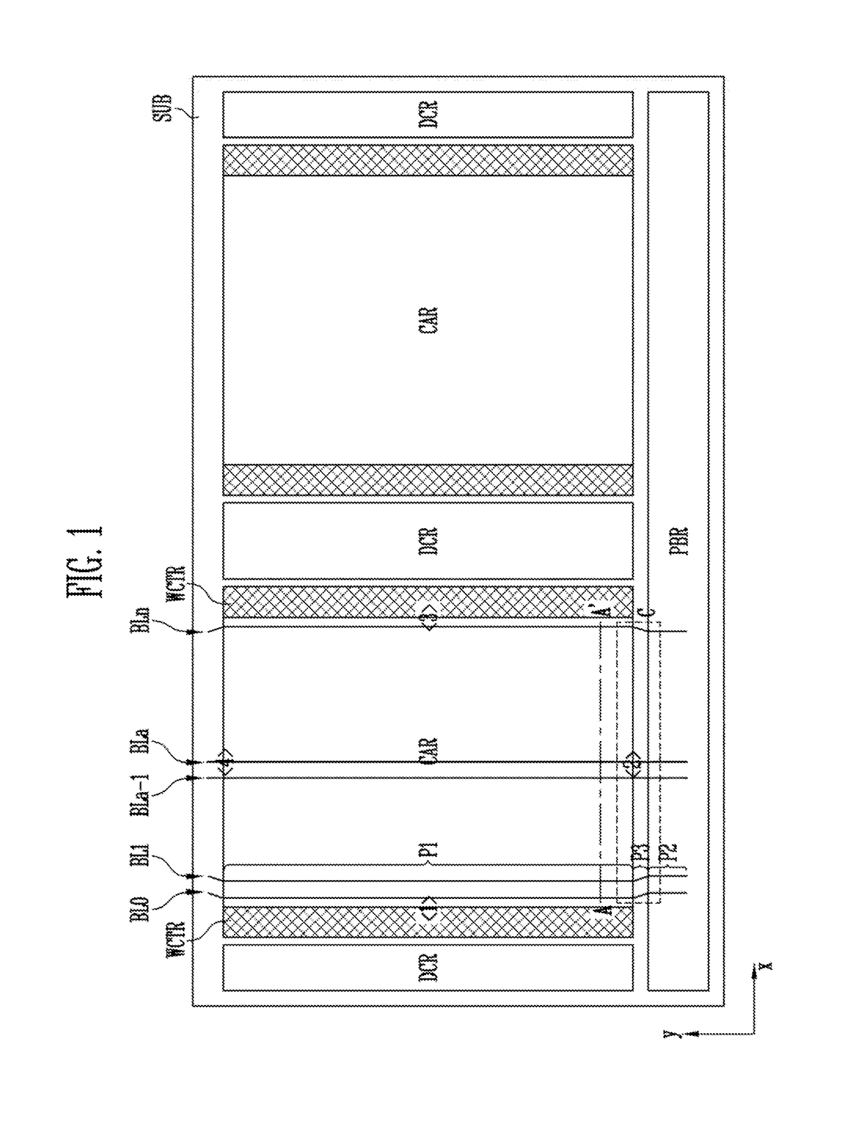
[0031]FIG. 1 is a diagram illustrating a semiconductor memory device according to an embodiment.

[0032]Referring to FIG. 1, a semiconductor memory device may include a cell array region CAR, a word line contact region WCTR, a decoding circuit region DCR, and a page buffer region PBR.

[0033]A cell array may be located in the cell array region CAR, and memory cells for storing data may be fo...


PUM


Abstract

A semiconductor memory device includes a cell array region formed on a substrate, a word line contact region, and a page buffer region coupled to the cell array region through bit lines, wherein at least one of the bit lines has a curved structure toward the word line contact region. According to an embodiment, a misalignment between a cell plug and a contact plug caused by a natural cell plug bending phenomenon may be reduced to improve operational reliability of a semiconductor memory device.

Description

CROSS-REFERENCE TO RELATED APPLICATION[0001]The present application claims priority under 35 U.S.C. § 119(a) to Korean patent application number 10-2016-0146710, filed on Nov. 4, 2016, the entire disclosure of which is incorporated herein by reference in its entirety.BACKGROUNDField of Invention[0002]Various embodiments of the invention relate generally to a semiconductor memory device, and more particularly, to a semiconductor memory device capable of improving operational reliability.Description of Related Art[0003]Semiconductor memory devices may include a plurality of memory cells capable of storing data.[0004]Three-dimensional semiconductor memory devices including three-dimensionally arranged memory cells have been proposed for achieving a higher degree of integration.[0005]A three-dimensional semiconductor memory device may include interlayer insulating layers and word lines stacked alternately with each other, and channel layers formed in channel holes passing therethrough. ...

Claims


Application Information

Patent Timeline
IPC IPC(8): H01L27/11582H01L27/11568H01L23/522H01L27/11573H01L23/528
CPCH01L27/11582H01L27/11568G11C16/06H01L27/11573H01L23/5283H01L23/5226H10B41/40H10B41/20H10B43/40H10B43/20G11C5/025G11C7/18G11C16/0466H10B43/10H10B43/35H10B43/50H10B43/27H10B41/50H10B41/27H10B43/30
Inventor KIM, YUNG JUNKIM, SUK GOO
Owner SK HYNIX INC
Why Eureka
Try Eureka