Drive circuit of display device

a display device and drive circuit technology, applied in the direction of digital storage, optics, instruments, etc., can solve problems such as tft malfunctions, and achieve the effects of preventing malfunctions of drive circuits, stabilizing potentials, and reducing influen

Inactive Publication Date: 2018-05-31
SHARP KK
View PDF0 Cites 5 Cited by
  • Summary
  • Abstract
  • Description
  • Claims
  • Application Information

AI Technical Summary

Benefits of technology

[0019]According to the first aspect of the present invention, it as possible to stabilize a potential of the light-shielding film using the auxiliary capacitor formed between the light-shielding film, and the electrode member, and reduce an influence which the light-shielding film exerts on the thin film transistor. Therefore, it is possible to prevent malfunction of the drive circuit due to a provision of the light-shielding film. Furthermore, since the light-shielding film is electrically isolated, it is not necessary to provide a wiring for supplying a potential to the light-shielding film and a contact hole for connecting the wiring and the light-shielding film. Therefore, it is possible to prevent an increase in a circuit area and a complication of a manufacturing process. Consequently, it is possible to provide a small-area and low-cost drive circuit of a display device, the drive circuit including a light-shielded thin film transistor.
[0020]According to the second aspect of the present invention, it is possible to stabilize the potential of the light-shielding film and reduce an off-leakage current due to the provision of the light-shielding film, by fixedly applying; the off potential of the thin film transistor to the electrode member which is one electrode of the auxiliary capacitor. Furthermore, by reducing the off-leakage current, it is possible to prevent the malfunction of the drive circuit due to the provision of the light-shielding film when the thin film transistor is in an off state and the second conduction electrode is in a floating state.
[0021]According to the third aspect of the present invention, the auxiliary capacitor for stabilizing the potential of the light-shielding film can be formed, using the electrode member formed integrally with the first conduction electrode of the thin film transistor.
[0022]According to the fourth aspect of the present invention, the auxiliary capacitor for stabilizing the potential of the light-shielding film can be formed, using the electrode member formed in the same layer as the channel portion of the thin film transistor and electrically connected to the first conduction electrode of the thin film transistor.
[0023]According to the fifth aspect of the present invention, the auxiliary capacitor can be formed without exerting a large influence on a layout of other parts, by forming the electrode member between the first and second conduction electrodes.
[0024]According to the sixth aspect of the present invention, it is possible to apply, to the electrode member, an off potential fixedly applied to the one conduction electrode of the other thin film transistor, stabilize the potential of the light-shielding film, and reduce the off-leakage current due to the provision of the light-shielding film, by electrically connecting the electrode member to the one conduction electrode of the other thin film transistor. Furthermore, by reducing the off-leakage current, it is possible to prevent the malfunction of the drive circuit due to the provision of the light-shielding film when the thin film transistor is in the off state and the second conduction electrode is in the floating state.

Problems solved by technology

When the light-shielding film is provided to the TFT, the channel portion of the TFT may be influenced by a potential of the light-shielding film and the TFT may malfunction.

Method used


Image

  • Drive circuit of display device
  • Drive circuit of display device
  • Drive circuit of display device

Examples


first embodiment

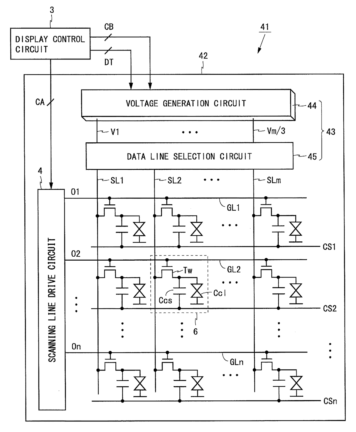
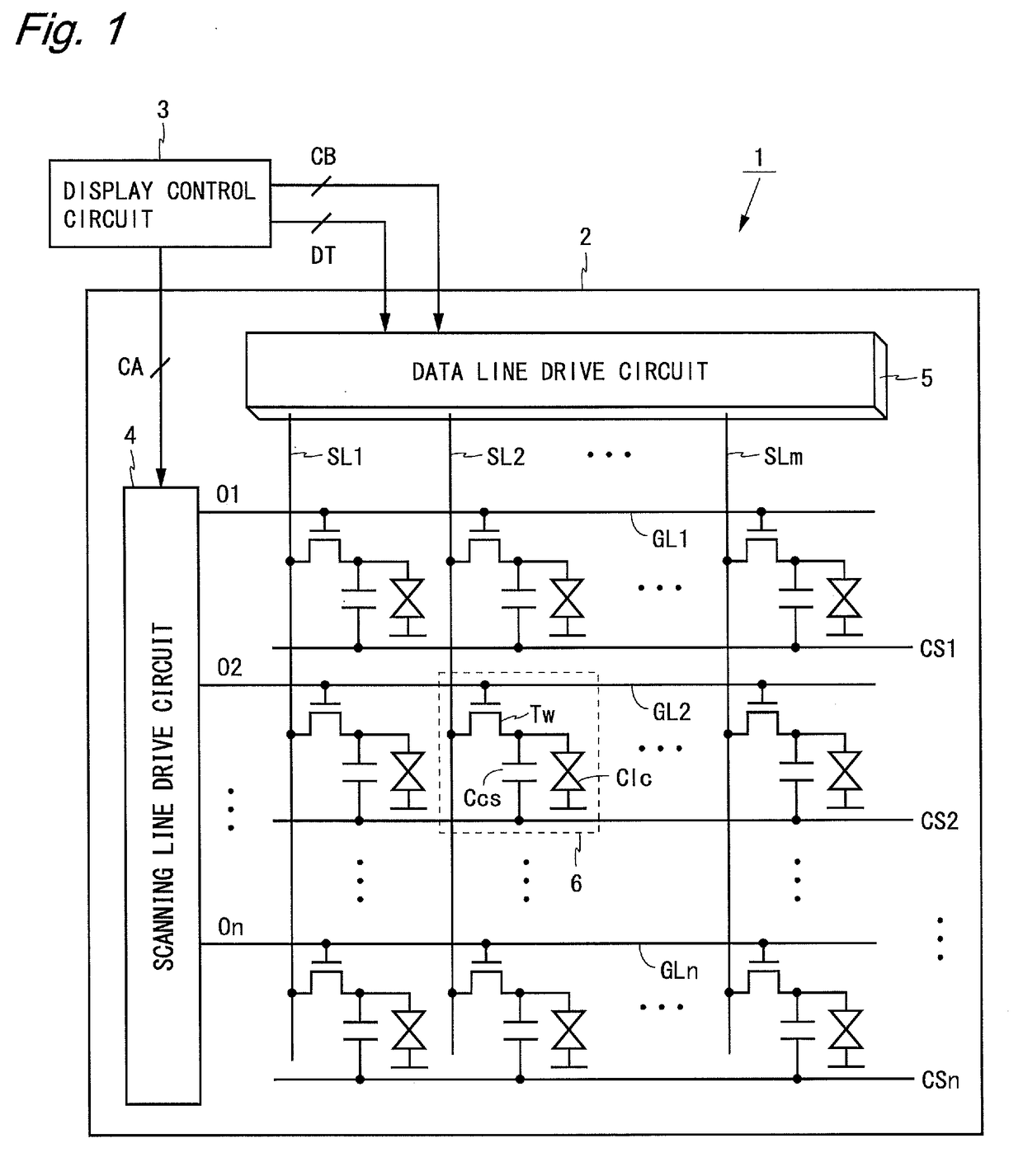
[0050]FIG. 1 is a block diagram showing a configuration of a liquid crystal display device including a scanning line drive circuit according to a first embodiment of the present invention. A liquid crystal display device 1 shown in FIG. 1 includes a liquid crystal panel 2, a display control circuit 3, a scanning line drive circuit 4, and a data line drive circuit 5.

[0051]The liquid crystal panel 2 includes n scanning lines GL1 to GLn, m data lines SL1 to SLm, n storage capacitance lines CS1 to CSn, and (m×n) pixel circuits 6. The scanning lines GL1 to GLn are arranged in parallel to each other. The data lines SL1 to SLm are arranged in parallel to each other so as to intersect with the scanning lines GL1 to GLn perpendicularly. The scanning lines GL1 to GLn and the data lines SL1 to SLm intersect at (m×n) points. The (m×n) pixel circuits 6 are arranged near intersections of the scanning lines GL1 to GLn and the data lines SL1 to SLm. The storage capacitance lines CS1 to CSn are arra...

second embodiment

[0087]A scanning line drive circuit according to a second embodiment of the present invention is different from that according to the first embodiment in a method of forming the auxiliary capacitor C2. In the present embodiment, the electrode member is formed in a same layer as the channel portion of the protection target transistor, and is electrically connected to the first conduction electrode of the protection target transistor. Differences from the first embodiment will be described below.

[0088]FIG. 9 is a layout diagram of the transistor Tr4 and its neighborhood in a scanning line drive circuit according to a first example of the present embodiment. In the first example, in order to form the auxiliary capacitor C2, an electrode member 22 is formed integrally with the semiconductor portion 16 in the semiconductor layer. A semiconductor layer pattern has a shape shown in FIG. 10. The extension portion 20 of the light-shielding film 12 and the electrode member 22 are formed so as...

third embodiment

[0092]A scanning line drive circuit according to a third embodiment of the present invention is different from those according to the first and second embodiments in a method of forming the auxiliary capacitor C2. In the present embodiment, the electrode member is electrically connected to one conduction electrode of a transistor other than the protection target transistor. Differences from the first and second embodiments will be described below.

[0093]FIGS. 13 to 15 are layout diagrams of the transistor Tr4 and its neighborhood in scanning line drive circuits according to first to third examples of the present embodiment, respectively. In FIGS. 13 to 15, a conduction electrode 31 is either a drain electrode or a source electrode of another transistor. The off potential of the transistor is fixedly applied to the conduction electrode 31. The conduction electrode 31 and the semiconductor portion (not shown) of the other transistor are electrically connected using a contact hole 32.

[0...


PUM

PropertyMeasurementUnit
voltagesaaaaaaaaaa
threshold voltageaaaaaaaaaa
brightnessaaaaaaaaaa

Abstract

A drive circuit of a display device includes a TFT having a source electrode 15, a drain electrode 14, and a gate electrode 13. Provided is an electrically isolated light-shielding film 12 which has a main body portion for shielding a channel portion of the TFT, and an extension portion 20 formed integrally with the main body portion. An auxiliary capacitor C2 is formed by overlapping, in a planar view, the extension portion 20 with an electrode member 21 formed integrally with the source electrode 15. In place of the electrode member 21, an electrode member formed in a same layer as the channel portion and connected to the source electrode 15, an electrode member connected to one conduction electrode of another TFT, or an electrode member formed integrally with the gate electrode 13 may be used. With this, a small-area and low-cost drive circuit including a light-shielded thin film transistor is provided.

Description

TECHNICAL FIELD[0001]The present invention relates to a drive circuit of a display device, especially to a drive circuit of a display device, the drive circuit including a light-shielded thin film transistor.BACKGROUND ART[0002]An active-matrix type display device displays an image by selecting pixel circuits arranged two-dimensionally in units of row and writing voltages in accordance with image data to the selected pixel circuits. Thus, the display device is provided with a scanning line drive circuit for driving scanning lines and a data line drive circuit for driving data lines. Furthermore, a technology (driver monolithic technology) for integrally forming all or a part of the drive circuits on a display panel with the pixel circuits using a manufacturing process for forming a thin film transistor (hereinafter abbreviated as TFT) in the pixel circuit has been put into practical use.[0003]Unlike a transistor in a circuit included in an IC chip, the TFT formed on the display pane...

Claims


Application Information

Patent Timeline
Patent Type & Authority Applications(United States)
IPC IPC(8): G02F1/1335G02F1/1368G02F1/1343G09G3/36
CPCG02F1/133512G02F1/1368G02F1/134336G09G3/3677G09G3/3688G09G2300/0426G09G2310/0286G09G2310/08G09G3/3648G09G3/3674G09G2300/0876G11C19/28H01L29/786G09G3/20G09G3/36
Inventor YAMAGUCHI, TAKAHIROFURUTA, SHIGEYAMADA, JUNICHIYAMANAKA, HIDEKAZUMURAKAMI, YUHICHIROHSASAKI, YASUSHI
Owner SHARP KK
Why Eureka
Try Eureka