Light emitting diode display

a technology of light-emitting diodes and leds, applied in the field of display, can solve the problems of inconsistent luminous efficiency of leds of different colors, low blue luminous efficiency of leds, and instability of organic light-emitting materials, so as to improve improve the inconsistent luminous efficiency of sub-pixels. , the effect of improving the inferior luminous efficiency of micro leds

Inactive Publication Date: 2018-06-07
AU OPTRONICS CORP
View PDF14 Cites 11 Cited by
  • Summary
  • Abstract
  • Description
  • Claims
  • Application Information

AI Technical Summary

Benefits of technology

[0012]Since the red micro LED has an inferior luminous efficiency to the green micro LED, the total area of the light-exiting surfaces of the red micro LEDs is larger than the total area of the light-exiting surfaces of the green micro LEDs to improve the inferior luminous efficiency of the red micro LED according to the embodiments of the disclosure. In addition, as compared with green light, human eyes are less sensitive to red light. Hence, when the total area of the light-exiting surfaces of the red micro LEDs are larger, the problem that human eyes are not easy to perceive red light can be improved so as to improve the inconsistent luminous efficiencies of sub-pixels of different colors.

Problems solved by technology

However, the OLED displays have a low blue luminous efficiency, and the organic light emitting materials have the stability problem which are the major problems faced in mass production.
However, after LEDs are shrunk down to a micrometer scale, the luminous efficiencies of the LEDs of different colors are not consistent.
Hence, users may find that light in some wave band is too bright and light in some other wave band is too dark, thus hindering the development of LED displays.

Method used


Image

  • Light emitting diode display
  • Light emitting diode display
  • Light emitting diode display

Examples


Embodiment Construction

[0024]In the following detailed description, for purposes of explanation, numerous specific details are set forth in order to provide a thorough understanding of the disclosed embodiments. It will be apparent, however, that one or more embodiments may be practiced without these specific details. In addition, drawings are only for the purpose of illustration and not plotted according to the original size. Wherever possible, the same reference numbers are used in the drawings and the description to refer to the same or like parts.

[0025]As used herein, “substantially”, “around,”“about” or “approximately” shall generally mean within 20 percent, preferably within 10 percent, and more preferably within 5 percent of a given value or range. Numerical quantities given herein are approximate, meaning that the term “substantially”, “around,”“about” or “approximately” can be inferred if not expressly stated.

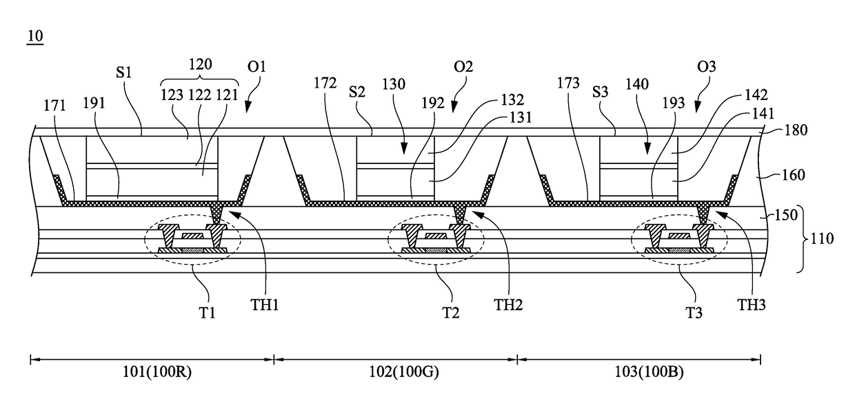
[0026]In the following embodiments, a light emitting diode (LED) display comprises a plu...


PUM


Abstract

A light emitting diode (LED) display includes a substrate, a pixel define layer, at least one first color micro LED, and at least one second color micro LED. The pixel define layer is disposed on the substrate and has a first opening and a second opening separated from each other. Contours of the first and second openings on a surface of the pixel define layer facing away from the substrate respectively define areas which are the same as each other. The first color micro LED is disposed in the first opening and has a first vertical projection projected on the substrate. The second color micro LED is disposed in the second opening and has a second vertical projection projected on the substrate. An area of the first vertical projection is different from an area of the second vertical projection.

Description

RELATED APPLICATIONS[0001]The present application is a continuation of U.S. application Ser. No. 15 / 158,725, filed May 19, 2016, and the application claims priority to Taiwan Application Serial Number 104119432, filed Jun. 16, 2015, which are incorporated herein by reference in its entirety.BACKGROUNDField of Disclosure[0002]The present disclosure relates to a display. More particularly, the disclosure relates to a light emitting diode (LED) display and a manufacturing method thereof.Background of the Disclosure[0003]With the progress of technology, displays have gradually changed from the bulky cathode ray tube (CRT) displays to the flat, lightweight and slim liquid crystal displays (LCDs), plasma display panels (PDPs), or organic light emitting diode (OLED) displays, etc.[0004]The OLED displays, as compared with the LCDs, do not need color filters as required by traditional LCD displays, thus having a simpler structure and smaller volume. In addition to that, OLEDs can be fabricat...

Claims


Application Information

Patent Timeline
Patent Type & Authority Applications(United States)
IPC IPC(8): H01L27/12G09G3/32G09G3/20
CPCG09G2320/0666G09G2320/0242G09G2300/0452G09G2300/0443H01L27/1259G09G3/32G09G3/2003H01L25/0753G09G2300/0426H01L21/77H01L27/156
Inventor CHANG, CHENG-CHIEHWU, TSUNG-TIENLIU, KANG-HUNGHSIAO, HSIANG-YUN
Owner AU OPTRONICS CORP
Why Eureka
Try Eureka