Optical semiconductor device and process for producing the same
Inactive Publication Date: 2006-08-01
RENESAS ELECTRONICS CORP
View PDF11 Cites 4 Cited by
Summary
Abstract
Description
Claims
Application Information
AI Technical Summary
This helps you quickly interpret patents by identifying the three key elements:
Problems solved by technology
Method used
Benefits of technology
Benefits of technology
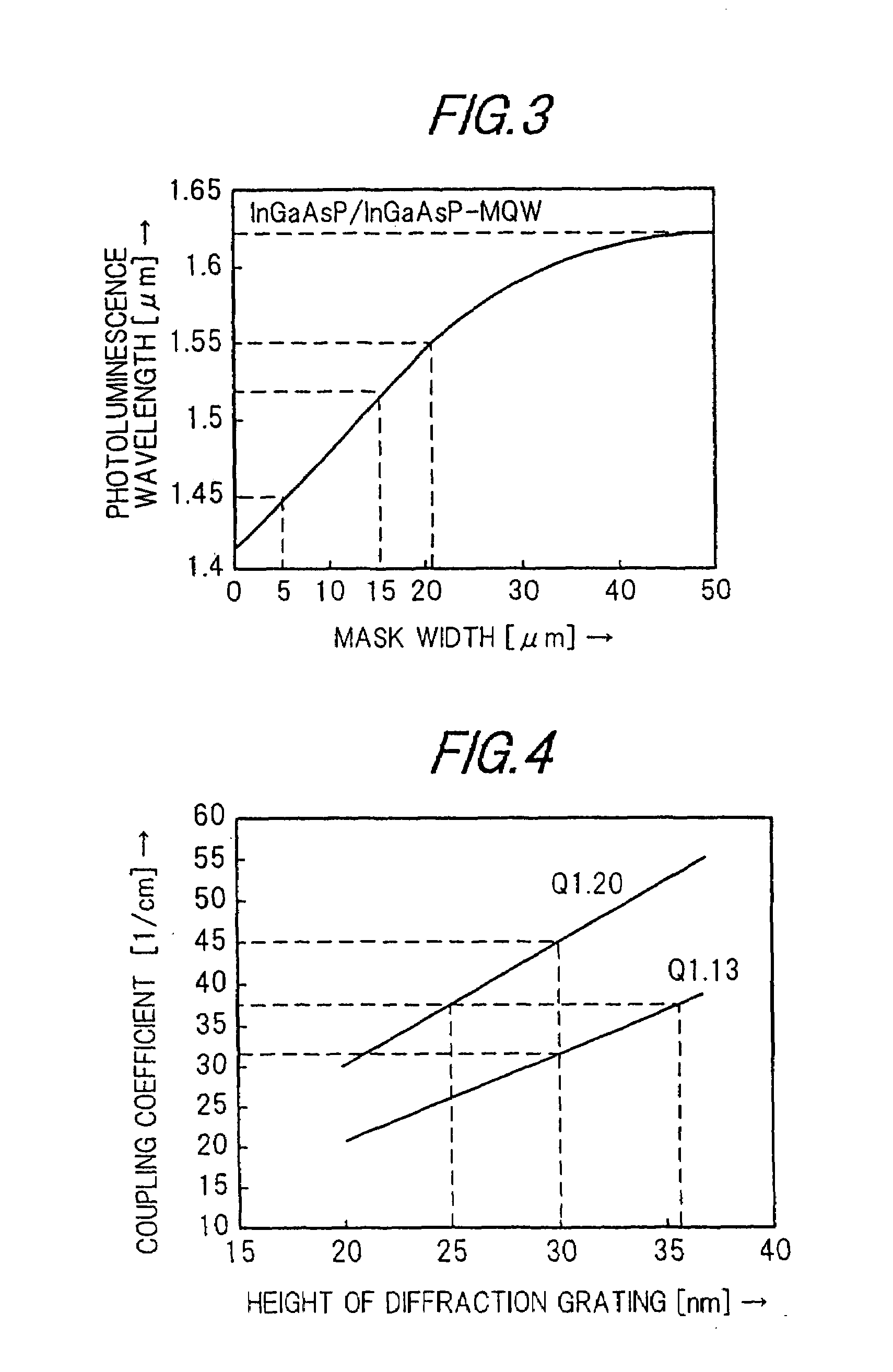
[0025]According to this production process, in forming a plurality of semiconductor lasers with a plurality of diffraction gratings on a substrate, the height of each diffraction grating is set so that the coupling coefficient is identical for the semiconductor lasers, followed by the formation of laser active layers respectively on the diffraction gratings. By virtue of the control of the height of the diffraction gratings, for the diffraction
Problems solved by technology
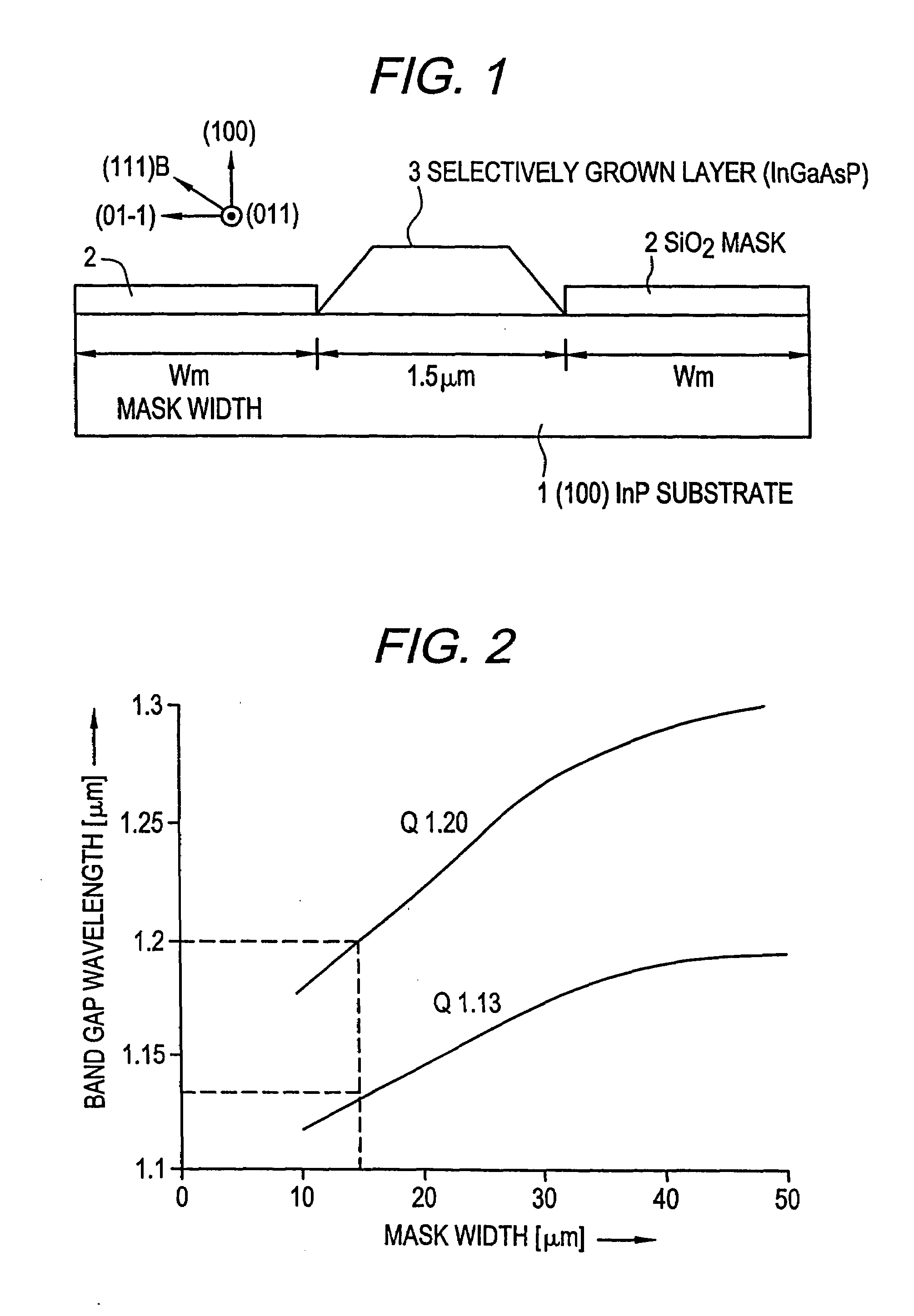
The preparation of the active layer by selective MOVPE, however, leads to a change in band gap wavelength of the optical guide layer formed on the diffraction grating and, in addition, a change in thickness of the active layer.
This results in a change in light intensity in the diffraction grating region.
According to the conventional optical semiconductor device and production proce
Method used
Image
Click on the blue label to locate the original text in one second.
Reading with bidirectional positioning of images and text.
Examples
first preferred embodiment
[0082]Next, the production process of an optical semiconductor device according to the invention will be explained in conjunction with the accompanying drawings.
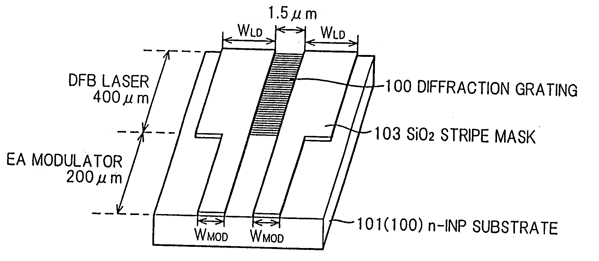
[0083]FIGS. 12, 13, 14, 15, 16, 17, 18, 19, 20, 21, and 22 show the first preferred embodiment of the invention. The first preferred embodiment is an example of an integration product of DFB lasers and EA modulators with different wavelengths. FIG. 12 shows a production process of an optical semiconductor device according to the invention, FIG. 13 illustrates the formation of a plurality of diffraction gratings on a substrate, wherein OF represents an orientation flat (this is true of FIG. 16), FIG. 14 shows the relationship between the resist opening width WE and the DFB oscillation wavelength, FIG. 15 shows the relationship between the drawing pitch and the DFB oscillation wavelength, FIG. 16 shows SiO2 stripe masks patterned according to diffraction gratings, FIG. 17 shows the details of the SiO2 stripe mask and one devic...
second preferred embodiment
[0095]A production process, wherein only DFB lasers with different wavelengths and free from EA modulators with different wavelengths are simultaneously formed on a substrate, will be explained as the second preferred embodiment of the invention with reference to FIGS. 26, 27, 28, 29, and 30.
[0096]FIG. 26 illustrates the formation of diffraction gratings, FIG. 27 illustrates patterning using stripe masks after the state shown in FIG. 26, FIG. 28 shows the arrangement of a mask pattern in one device, FIG. 29 is a cross-sectional view taken on line D–D′ of FIG. 28, and FIG. 30 illustrates the patterning of a p electrode.
[0097]According to this preferred embodiment, as with the first preferred embodiment, diffraction gratings are formed by electron beam exposure and etching. At that time, as shown in FIG. 26, a plurality of diffraction gratings 200 are formed in all the regions in the direction of [011] of the substrate 201, and a pattern of diffraction gratings repeated at pitches of ...
PUM
Abstract
A resist is coated on a substrate. The resist is exposed to a pattern of a plurality of diffraction gratings for setting pitches corresponding respectively to oscillation wavelengths for the plurality of semiconductor lasers and for setting heights of the diffraction gratings which provide an identical coupling coefficient independently of the oscillation wavelengths. The coating is etched in such a manner that the level of etching per unit time is identical. A stripe mask is patterned according to the arrangement of the diffraction gratings. A laser active layer is formed on each of the diffraction gratings by selective MOVPE growth. An electrode is formed on each of the laser active layer on its top surface and the backside of the substrate. By virtue of this constitution, an optical semiconductor device and a process for producing the same can be realized which, when a plurality of semiconductor lasers are simultaneously formed on a single semiconductor substrate, can prevent a variation in coupling coefficient.
Description
[0001]This is a divisional of application Ser. No. 09 / 721,662, filed Nov. 27, 2000; the disclosure of which is incorporated herein by reference now U.S. Pat. No. 6,707,839.FIELD OF THE INVENTION[0002]The invention relates to an optical semiconductor device and a process for producing the same. More particularly, the invention relates to an optical semiconductor device for use in WDM (wavelength division multiplexing) transmission, comprising a plurality of semiconductor lasers with different oscillation wavelengths which have been simultaneously formed on a single substrate, and a process for producing the same.BACKGROUND OF THE INVENTION[0003]In recent years, attention has been drawn to optical communication as means for coping with a rapidly increasing demand for communication. In this connection, a WDM optical communication system has attracted attention, because this system can transmit optical signals with different wavelengths over a single optical fiber to realize high capaci...
Claims
Application Information
Patent Timeline
Application Date:The date an application was filed.
Publication Date:The date a patent or application was officially published.
First Publication Date:The earliest publication date of a patent with the same application number.
Issue Date:Publication date of the patent grant document.
PCT Entry Date:The Entry date of PCT National Phase.
Estimated Expiry Date:The statutory expiry date of a patent right according to the Patent Law, and it is the longest term of protection that the patent right can achieve without the termination of the patent right due to other reasons(Term extension factor has been taken into account ).
Invalid Date:Actual expiry date is based on effective date or publication date of legal transaction data of invalid patent.

