
Display device and electronic apparatus

a technology of electronic equipment and display device, which is applied in the direction of discharge tube/lamp details, lamp details, instruments, etc., can solve the problems of increasing the thickness of the panel module, difficult to take advantage of the small thickness of the light-emitting display device, and difficulty in detecting the luminance of the dummy pixel, etc., to achieve efficient detection and increase the thickness

Inactive Publication Date: 2013-07-23
JOLED INC
View PDF10 Cites 4 Cited by
  • Summary
  • Abstract
  • Description
  • Claims
  • Application Information

AI Technical Summary

Benefits of technology

[0011]Thus, it is desirable to provide a display device that, when a photodetector is provided on the opposite side of a display panel from the light-emitting surface, allows efficient detection of the dummy pixel luminance; and an electronic apparatus including the display device.
[0013]In the display device thus configured, the photodetector is provided on the opposite side of the display panel from the light-emitting surface thereof, for example, on the rear side of the display panel. As a result, because a driver module for driving a pixel on the display panel is present on the rear side of the display panel, the panel module does not have increased thickness. Further, light emitted from the dummy pixel is reflected from the reflection film and thereby directed to the photodetector. As a result, even though the photodetector is provided on the rear side of the display panel, the luminance of the dummy pixel can be efficiently detected.
[0014]According to the embodiment of the invention, even when the photodetector is positioned on the opposite side of a display panel from the light-emitting surface thereof, the luminance of the corresponding dummy pixel can be efficiently detected.

Problems solved by technology

In such a case where a photodetector is positioned on the front side of a display panel, the panel module has increased thickness, and it thus is difficult to take advantage of the small thickness of the light-emitting display device.
Because of the darker environment as compared with detection on the light-emitting-surface side, it is difficult to detect the dummy pixel luminance.

Method used


Image

  • Display device and electronic apparatus
  • Display device and electronic apparatus
  • Display device and electronic apparatus

Examples


example 1

[2-2. Example 1]

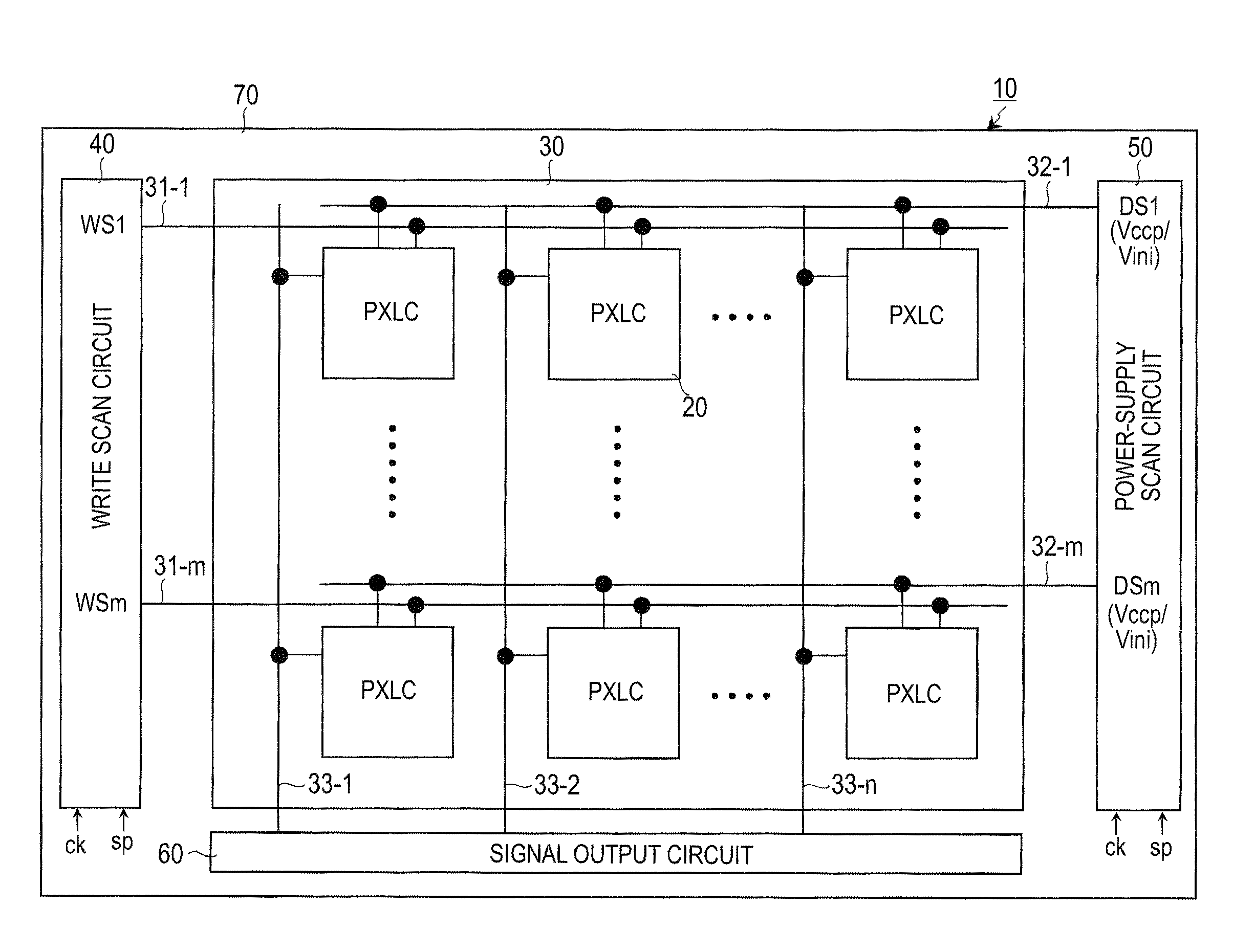
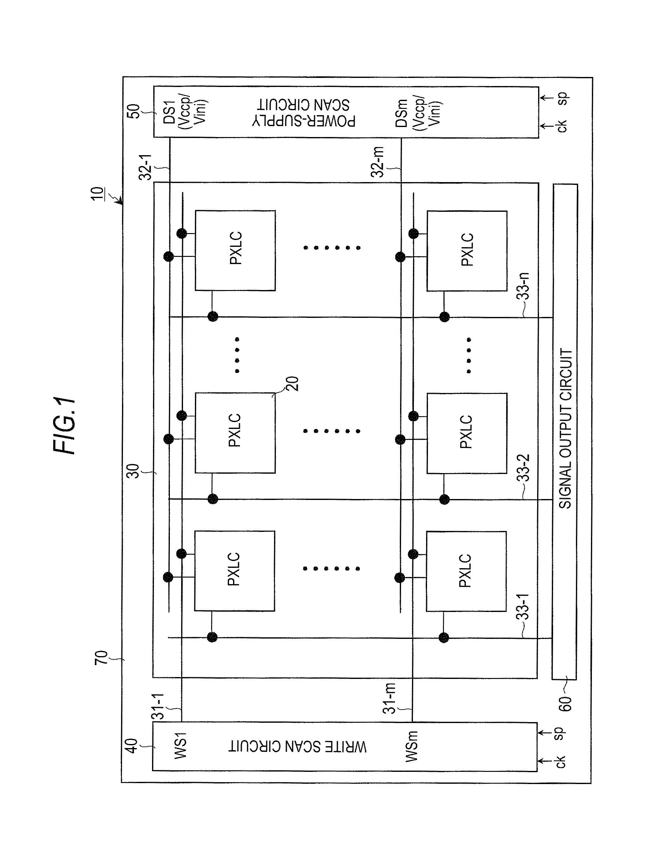
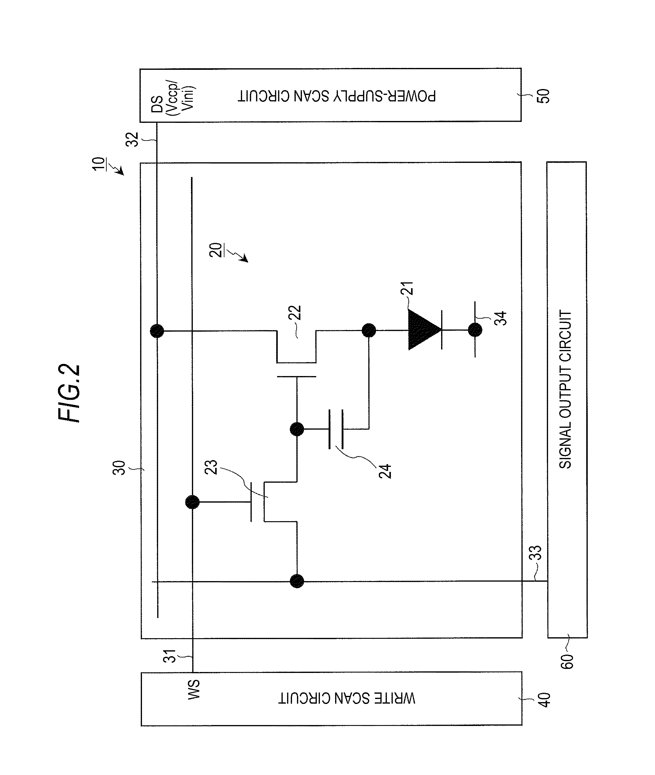
[0138]FIG. 11 is a cross section showing the configuration of a dummy pixel 811 including a photodetector 812 according to Example 1. As mentioned above, like the pixel (effective pixel) 20 shown in FIG. 2, the dummy pixel 811 includes an organic EL device 21, and also has a drive circuit including a drive transistor 22 and the like.

[0139]As shown in FIG. 11, the drive circuit including the drive transistor 22 and the like is formed on a transparent substrate, for example, a glass substrate, 701. Among the components of the drive circuit, only the drive transistor 22 is illustrated in the figure, omitting other components.

[0140]The drive transistor 22 includes a gate electrode 221, source / drain regions 223 and 224 on the opposite sides of a polysilicon semiconductor layer 222, and a channel-forming region 225 in a portion of the polysilicon semiconductor layer 222 facing the gate electrode 221. Source / drain electrodes 226 and 227 are electrically connected to the sou...

example 2

[2-3. Example 2]

[0156]FIG. 13 is a cross section showing the configuration of a dummy pixel 811 including a photodetector 812 according to Example 2. In FIG. 13, the components common to FIG. 11 (corresponding components) are indicated by the same reference numerals, and will not be further explained to avoid repetitive description.

[0157]In the layout of the photodetector 812 of Example 1, the photodetector 812 is provided by attachment on the rear side of the display panel 70, for example. In contrast, in the layout of the photodetector 812 of Example 2, as shown in FIG. 12, the photodetector 812 is provided by incorporation into the display panel 70 (built-in).

[0158]That is, in the layout of the photodetector 812 of Example 2, in the process of forming the drive transistor 22 and the like on the glass substrate 701, the photodetector 812 is also formed on the glass substrate 701 in the same manner. A PIN photodiode or the like is usable as such a photodetector 812.

[0159]The layout...

application example

4. Application Example

[0161]The display devices according to the embodiments of the invention explained above are applicable as display devices for use in an electronic apparatus of any field, where video signals supplied to the electronic apparatus or video signals produced in the electronic apparatus are displayed as images or videos. For example, the display devices can be applied for use in the various kinds of electronic apparatuses shown in FIGS. 14, to 18, such as a digital camera, a laptop personal computer, a mobile phone, and like portable terminals, a video camera and like display devices, etc.

[0162]Use of a display device according to an embodiment of the invention as a display device in an electronic apparatus of any field allows the electronic apparatus to achieve high-quality image display without an increase in size. That is, as is clear from the above-described embodiments, a display device according to an embodiment of the invention makes it possible to suppress bu...


PUM


Abstract

A display device includes: a dummy pixel provided on a display panel; a reflection film provided on a light-emitting-surface side of the display panel for reflecting light emitted from the dummy pixel; a photodetector provided on an opposite side of the display panel from the light-emitting surface for detecting the light emitted from the dummy pixel and reflected from the reflection film; and a correction circuit for correcting, based on the results of detection by the photodetector, the luminance of effective pixels that contribute to image display.

Description

BACKGROUND OF THE INVENTION[0001]1. Field of the Invention[0002]The present invention relates to a display device and an electronic apparatus. The invention particularly relates to a flat-panel display device including pixels that are arranged two-dimensionally in a matrix and have electro-optic devices; and also to an electronic apparatus including the display device.[0003]2. Description of the Related Art[0004]In recent years, in the field of display devices for displaying images, a flat-panel, light-emitting display device has been spreading rapidly. In such a light-emitting display, pixels (pixel circuits) having devices of a light-emitting type (light-emitting devices) as electro-optic devices are arranged in a matrix. A known light-emitting device is an EL (Electro Luminescence) device that uses the phenomenon of light emission in response to the application of an electric field to an organic thin film. An organic EL device is an electro-optic device of a so-called current-dri...

Claims


Application Information

Patent Timeline
Patent Type & Authority Patents(United States)
IPC IPC(8): G09G3/30
CPCG09G3/3233G09G2320/029G09G2320/043G09G2320/046G09G2360/145G09G2360/16H10K59/60H10K59/121
Inventor YAMASHITA, JUNICHIUCHINO, KATSUHIDE
Owner JOLED INC
Learn More