Logic circuit based on thin film transistor
- Summary
- Abstract
- Description
- Claims
- Application Information
AI Technical Summary
Benefits of technology
Problems solved by technology
Method used
Image

Examples
example i
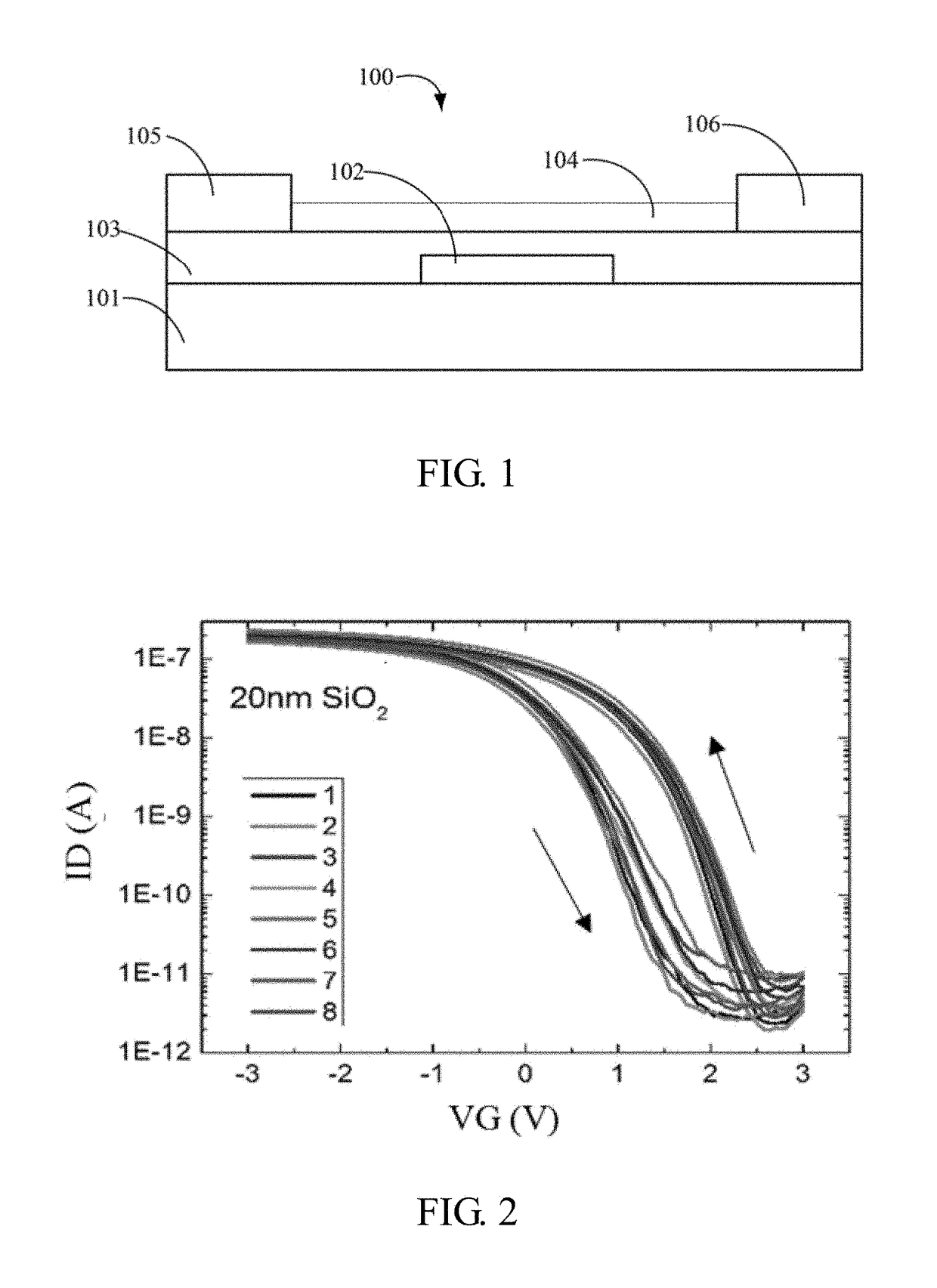
[0054]Referring to FIG. 1, in example I, a thin film transistor 100 is provided. The thin film transistor 100 is back-gate type and includes a substrate 101, a gate 102, a dielectric layer 103, a semiconductor layer 104, a source 105, and a drain 106. The gate 102 is located on a surface of the substrate 101. The dielectric layer 103 is located on the substrate 101 and covers the gate 102. The semiconductor layer 104 is located on a surface of the dielectric layer 103 and spaced apart from the gate 102. The source 105 and the drain 106 are located on the dielectric layer 103, spaced apart from each other, and electrically connected to the semiconductor layer 104. A channel is formed between the source 105 and the drain 106 by the semiconductor layer 104. The semiconductor layer 104 includes a first surface on one side of the semiconductor layer 104 and a second surface on opposite side of the semiconductor layer 104, the first surface is in direct contact with the dielectric layer 1...
example ii
[0069]Referring to FIG. 7, in example II, a thin film transistor 100A is provided. The thin film transistor 100A is top-gate type and includes a substrate 101, a gate 102, a dielectric layer 103, a semiconductor layer 104, a source 105, and a drain 106. The semiconductor layer 104 is located on a surface of the substrate 101. The source 105 and the drain 106 are located on the substrate 101, spaced apart from each other, and electrically connected to the semiconductor layer 104. A channel is formed between the source 105 and the drain 106 by the semiconductor layer 104. The dielectric layer 103 is located on a surface of the semiconductor layer 104 and covers the semiconductor layer 104, the source 105, and the drain 106. The gate 102 is located on a surface of the dielectric layer 103 and spaced apart from the semiconductor layer 104.
[0070]The thin film transistor 100A in example II is similar to the thin film transistor 100 in example I except that the thin film transistor 100A is...
example iii
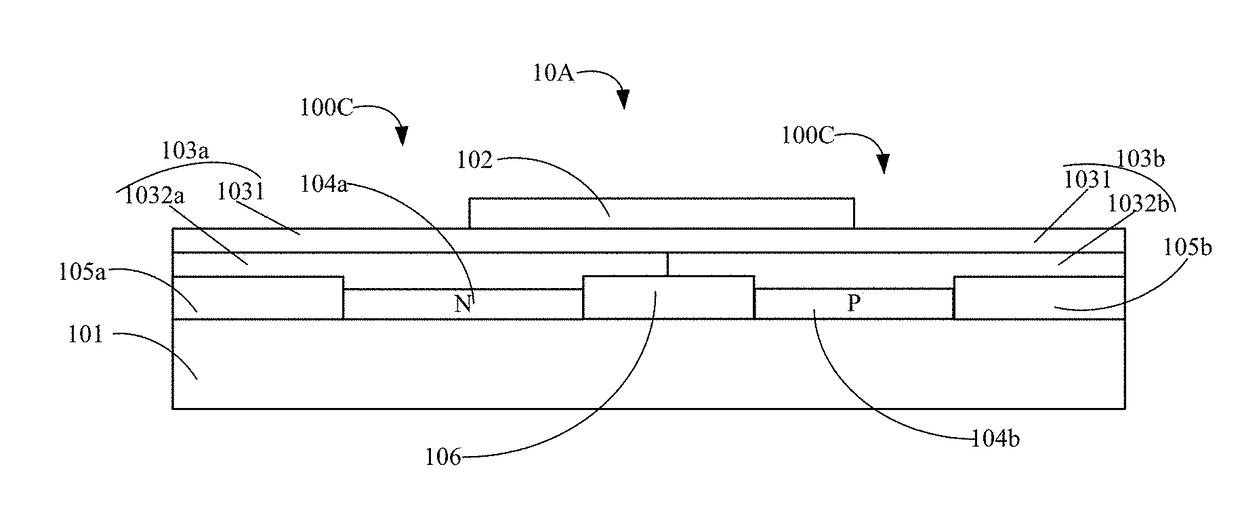
[0080]Referring to FIG. 11, in example III, a thin film transistor 100B is provided. The thin film transistor 100B is back-gate type and includes a substrate 101, a gate 102, a dielectric layer 103, a semiconductor layer 104, a source 105, and a drain 106. The gate 102 is located on a surface of the substrate 101. The dielectric layer 103 is located on the substrate 101 and covers the gate 102. The semiconductor layer 104 is located on a surface of the dielectric layer 103. The source 105 and the drain 106 are located on the dielectric layer 103, spaced apart from each other, and electrically connected to the semiconductor layer 104. A channel is formed between the source 105 and the drain 106 by the semiconductor layer 104.
[0081]The thin film transistor 100B in example III is similar to the thin film transistor 100 in example I except that the dielectric layer 103 is a double-layer structure and includes a first sub-dielectric layer 1031 and a second sub-dielectric layer 1032 stack...
PUM
 Abstract
Description
Claims
Application Information