Supercharge Your Innovation With Domain-Expert AI Agents!

Bootstrap diode emulator circuit

a diode emulator and diode technology, applied in the field of bootstrap diode emulator semiconductor circuits, can solve the problems of high reverse breakdown voltage, inconvenient initialization, and high requirements for diodes

Active Publication Date: 2018-06-14
MOSWAY TECH LTD
View PDF2 Cites 3 Cited by
  • Summary
  • Abstract
  • Description
  • Claims
  • Application Information

AI Technical Summary

Benefits of technology

The invention provides a bootstrap diode emulator circuit that includes a transistor device and a diodic device. The anode of the circuit is connected to the low side supply voltage node, while the cathode of the circuit is connected to the bootstrap supply voltage node. The transistor device is a high-voltage device, while the diodic device is a medium-voltage device. The diodic device has a minimum reverse breakdown voltage larger than a difference between the magnitude of the threshold voltage and the minimum voltage at the anode of the bootstrap diode emulator circuit. The transistor device can be a JFET device or a PMOS or NMOS device. The circuit can be integrated into an integrated circuit chip or a half-bridge driver circuit. The technical effect of the invention is to provide a reliable and efficient bootstrap diode emulator circuit that can improve the performance and reliability of various electronic devices and circuits.

Problems solved by technology

Generally, such integration requires a diode with high reverse breakdown voltage that is normally not available in typical integrated circuit process technology platforms.
In particular, the second problem means that proper initialization will be required before the high voltage half bridge integrated circuit can enter into normal functional modes.
Problematically, however, such a device is not readily available in most high voltage integrated circuit process platforms.

Method used


Image

  • Bootstrap diode emulator circuit
  • Bootstrap diode emulator circuit
  • Bootstrap diode emulator circuit

Examples


Embodiment Construction

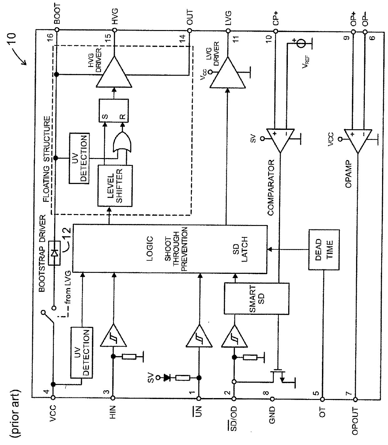
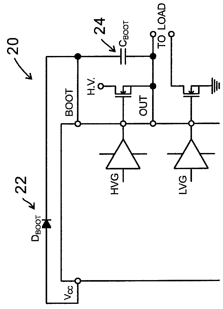
[0041]FIG. 3 shows a bootstrap diode emulator circuit 300 in one embodiment of the invention. The circuit 300 generally includes a transistor device 302 and a diodic device in the form of a switching device 306. The transistor device 302 is a high voltage JFET device. A source terminal of the JFET device 302 is connected with the switching device; a gate terminal of the JFET device 302 is connected to ground; a drain terminal of the JFET device 302 is connected to bootstrap supply voltage node BOOT. The switching device 306 is connected between low side supply voltage node VCC and the source terminal of the JFET device. In order to allow the full (maximum) voltage at node VCC to be passed to node BOOT, the magnitude of the pinch off voltage of the JFET device is larger than the maximum voltage at node VCC. In this embodiment, the switching device 306 connected at the source terminal is a medium voltage device. The minimum reverse breakdown voltage of the medium voltage device 306 is...


PUM


Abstract

A bootstrap diode emulator circuit having a cathode and an anode includes a transistor device and a diodic device. The transistor device is arranged at the cathode of the bootstrap diode emulator circuit. The diodic device has a cathode connected to the transistor device and an anode that is the anode of the bootstrap diode emulator circuit.

Description

TECHNICAL FIELD[0001]The invention relates to a bootstrap diode emulator circuit and in particular, but not exclusively, to a bootstrap diode emulator semiconductor circuit.[0002]BACKGROUND[0003]FIG. 1A shows a circuit diagram 10 of the L6390 high voltage half bridge driver integrated circuit manufactured by STMicroelectronics. As shown in FIG. 1A, the circuit 10 includes a built-in bootstrap diode 12 (labeled as “bootstrap driver”) arranged between the low side supply voltage node VCC and the bootstrap supply voltage node BOOT, for connection with a bootstrap capacitor (not shown). FIG. 1B illustrates circuit connection of part of the L6390 high voltage half bridge driver integrated circuit 10 with an external bootstrap diode DBOOT and other external electrical components for realizing a bootstrap driver.[0004]In the circuit 20 of FIG. 1B, during normal operation, energy is transferred from the low side power supply with nodes VCC and GND to high side supply decoupling capacitor CB...

Claims


Application Information

Patent Timeline
Patent Type & Authority Applications(United States)
IPC IPC(8): H03K17/567
CPCH03K17/567H03K17/063H03K17/6871H03K2217/0081H03K17/06H03K17/687H03K2017/307H03K2017/6875H03K2217/0018
Inventor CHAN, ON BON PETER
Owner MOSWAY TECH LTD
Features
  • R&D
  • Intellectual Property
  • Life Sciences
  • Materials
  • Tech Scout
  • Unparalleled Data Quality
  • Higher Quality Content
  • 60% Fewer Hallucinations
Learn More