Electrochemical deposition chamber

a technology of electrochemical and deposition chamber, which is applied in the direction of sealing devices, tanks, cells, etc., can solve the problems of reducing the number of electrolyte lost, complicating the pre and post deposition steps, and adding to the cost of electrolyte loss

Active Publication Date: 2018-06-21
SPTS TECH LTD
View PDF1 Cites 0 Cited by
  • Summary
  • Abstract
  • Description
  • Claims
  • Application Information

AI Technical Summary

Benefits of technology

[0043]tilting the chamber in order to assist in removing electrolyte from the housing through the fluid outlet pathway.

Problems solved by technology

While this reduces the number of times the edge seal / contact must be made it does complicate the pre and post deposition steps.
The challenge with this type of arrangement is to minimize the loss of electrolyte from the system as when the cell is opened and quantity of electrolyte flows over the edge of the wafer.
The lost electrolyte adds to cost (as it must be replaced) but also acts as a source of contamination for subsequent process steps.
Whilst a conventional clamshell type enclosure could be used in the type of arrangement there are significant costs associated with such an approach—not least the need for automated closure / opening of the clamshell and a further requirement for a seal between the clamshell and the electrolyte cavity.
Care must be also taken to ensure bubbles or trapped pockets of air / N2 / gas can readily leave the cell as these can have a detrimental effect on film uniformity.
However one of the key challenges for this type of low volume cell is to provide a means of removing the electrolyte from the cell in such a fashion that no electrolyte flows beyond the edge of front surface of the wafer when the cell is opened.
Whilst fluid removal may be aided for recycling purposes by small pipes, these will not be sufficient to avoid the in situ clean and the secondary containment region as relatively large amounts of fluid will remain on the wafer surface when the chamber is opened.
Also, the present inventors have realised that the use of tubes and pipes is undesirable, because they can interfere with dielectric properties of the chamber and they can impose restrictions on fluid removal rates.
Further, it is generally undesirable to obscure the substrate with a dielectric material.

Method used


Image

  • Electrochemical deposition chamber
  • Electrochemical deposition chamber
  • Electrochemical deposition chamber

Examples


Embodiment Construction

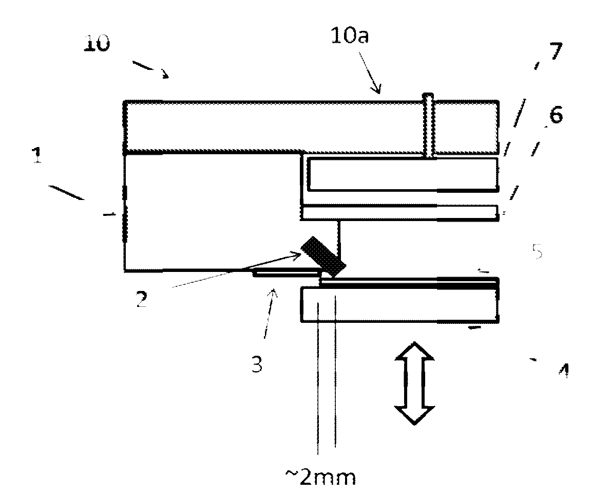
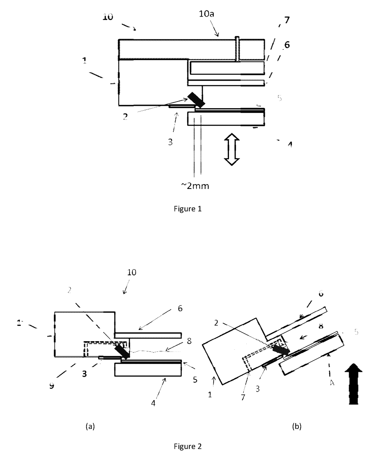
[0050]FIG. 1 shows a first embodiment of a chamber of the invention, depicted generally at 10. The chamber 10 is an electrochemical deposition chamber for processing a substrate 5. The substrate 5 is placed on a platen 4 either by hand or by mechanical means. The platen 4 is raised to compress an elastomeric seal 2 on the upper surface of the substrate 5 to form a fluid seal. At the same time as the fluid seal is being made, electrical contact is made with a seed layer on the upper surface of the substrate 5 by means of conductive springs 3. The seal 2 and conductive springs 3 are retained in a lower chamber body 1. As explained in more detail below, an advantage of the present invention is that it is possible to make contact within 1-2 mm of the edge of the substrate 5.

[0051]A soluble anode 7, which could be Cu or phosphorized Cu for Cu deposition, is located parallel with the wafer surface at or near to the top of the chamber 10. Electrical connections to the anode 7 and fluid con...


PUM

PropertyMeasurementUnit
diameteraaaaaaaaaa
separation distancesaaaaaaaaaa

Abstract

According to the invention a method of removing electrolyte from an electrochemical deposition or polishing chamber comprising the steps of: providing an electrochemical deposition or polishing chamber comprising a support for a substrate, the support having an in-use position; a housing having an interior surface and a fluid outlet pathway for removing electrolyte from the chamber, wherein the fluid outlet pathway includes one or more slots which extend into the housing from at least one slotted opening formed in the interior surface; a seal for sealing the housing to a peripheral portion of a surface of a substrate position on the support in its in-use position; and a tilting mechanism for tilting the chamber in order to assist in removing electrolyte from the housing through the fluid outlet pathway; using an electrolyte to perform an electrochemical deposition or polishing processing on a substrate positioned on the support in its in-use position; and tilting the chamber using the tilting mechanism in order to assist in removing electrolyte from the housing through the fluid outlet pathway.

Description

CROSS-REFERENCE TO RELATED APPLICATION[0001]The Application claims benefit from and is a Continuation-in-Part Application of U.S. patent application Ser. No. 14 / 218,051 filed Mar. 18, 2014, entitled ELECTROCHEMICAL DEPOSITION CHAMBER, which is hereby incorporated by reference in its entirety.FIELD[0002]This invention relates to an electrochemical deposition chamber, and to associated methods of electrochemical deposition. The invention applies also to electrochemical polishing.BACKGROUND[0003]Electrochemical deposition (ECD) is an important technique in the manufacture of semiconductor devices and components, hard disk drive fabrication, and other applications. With the recent growth of interest in 3D integration of wafers, there is a developing interest in providing conductive layers in through silicon vias (TSVs). One of the most promising candidates for depositing conductors in features greater than 1 micron in diameter and less than 10:1 aspect ratio is electrochemical depositio...

Claims


Application Information

Patent Timeline
Patent Type & Authority Applications(United States)
IPC IPC(8): C25D17/02C25D3/38C25D17/00C25F3/16C25F7/00
CPCC25D17/02C25D3/38C25D17/001C25D17/004C25F3/16C25F7/00C25D21/00
Inventor MACNEIL, JOHN
Owner SPTS TECH LTD
Why Eureka
Try Eureka