System, a tangent probe card and a probe head assembly for testing semiconductor wafter

Inactive Publication Date: 2018-06-21
LEUNG WING CHEUK
View PDF25 Cites 0 Cited by
  • Summary
  • Abstract
  • Description
  • Claims
  • Application Information

AI Technical Summary

Benefits of technology

[0016]The throughput of the tangent probe card according to the present utility model is higher than that of the conventional vertical probe cards or MEMS probe cards since there is no need to move the pointed pin/structure.
[0017]

Problems solved by technology

This confronts the traditional testing methods with many challenges, such as:alignment of the probe tip with the test target.
For example, if the probe tip 111′ fails to reach the top center of the Cu pillar 400 during touchdown, the resulting shear force applied onto the stress point may create fracture to the pillar.
When the diameter of the probe is decreased, the probe will be weakened and become more subjected to d

Method used


Image

  • System, a tangent probe card and a probe head assembly for testing semiconductor wafter
  • System, a tangent probe card and a probe head assembly for testing semiconductor wafter
  • System, a tangent probe card and a probe head assembly for testing semiconductor wafter

Examples


first embodiment

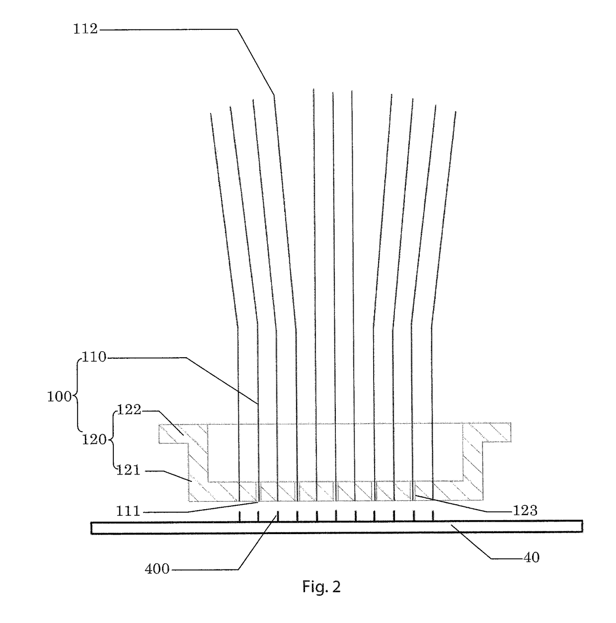
[0071]FIG. 5 is a perspective exploded view illustrating the first embodiment of the tangent probe card according to the utility model, where the plurality of probes are omitted for the sake of brevity. FIG. 6 is a bottom view of the tangent probe card according to the first embodiment. FIG. 7 is a cross-sectional view taken along the line A-A in FIG. 6. FIG. 8 is a top view of the tangent probe card according to the first embodiment, wherein the mounting hole of the upper holding block used to mount the spring is illustrated in a perspective view to show the location of the spring on the upper holding block. FIG. 9 is a cross-sectional view taken along the line B-B in FIG. 8, wherein “+” is utilized to denote the location of the spring behind the elastic ring since the spring is blocked by the elastic ring. Furthermore, the through-holes of the probe holding portion are not presented for the sake of clarity. FIG. 10 is a cross-sectional view illustrating wafer testing via the tange...

second embodiment

[0078]FIG. 11 is a perspective exploded view of the second embodiment of the tangent probe card according to the utility model, where the plurality of probes are omitted for the sake of brevity. FIG. 12 is a top view of the tangent probe card according to the second embodiment. FIG. 13 is a cross-sectional view taken along the line B-B in FIG. 12.

[0079]The second embodiment differs from the first embodiment in the fact that the buffer part 300 comprises an elastic ring only. In other words, the tangent probe card according to the second embodiment is not provided with a spring 320. The second embodiment will be detailedly described hereinafter.

[0080]In the second embodiment, the tangent probe card may comprise a probe head assembly with a probe holding portion 120, a holder 200 and an elastic ring 310. For the sake of clarity, the probes are not depicted in FIGS. 11-13. However, the probe head assembly may comprise a plurality of probes according to the above-mentioned embodiments. ...

third embodiment

[0083]FIG. 14 is a perspective exploded view illustrating the third embodiment of the tangent probe card according to the utility model, where the plurality of probes are omitted for the sake of brevity. FIG. 15 is a top view of the tangent probe card according to the third embodiment, wherein the mounting hole of the upper holding block that is used for mounting the spring is illustrated in a perspective view so as to show the location of the spring in the upper holding block. FIG. 16 is a cross-sectional view taken along the line B-B in FIG. 15.

[0084]The third embodiment 3 differs from the first embodiment in the fact that the buffer part 300 comprises the springs only. In other words, the tangent probe card according to the third embodiment is not provided with an elastic ring 310. The tangent probe card according to the third embodiment will be detailedly described hereinafter.

[0085]In the third embodiment, the tangent probe card may comprise a probe head assembly with a probe h...


PUM


Abstract

A system for semiconductor wafer testing, a tangent probe card and a probe head assembly thereof. The system has a tangent probe card and a tester. Testing ends of the probe card are flat, hence the allowable alignment budget will always be more generous for the tangent probe card. The probes are held on the probe head assembly, and once the alignment is achieved accurately during manufacture, the alignment will remain stable throughout the whole life cycle. The probe has a greater CCC due to its larger cross section. The throughput of the tangent probes is higher than that of the conventional probe card since there is no need to move the pointed pin/structure. No pointed pin/structure needs to be repaired, and the flat bottom surface of the probe head assembly is easier to clean and maintain.

Description

FIELD OF THE UTILITY MODEL[0001]The utility model relates to the technical field of semiconductor testing, and particularly, relates to a system for semiconductor wafer testing, a tangent probe card and a probe head assembly thereof.BACKGROUND OF THE UTILITY MODEL[0002]It is traditional, in the technical field of semiconductor wafer testing, to utilize a probe card as an interface between a tester and a semiconductor wafer. As shown in FIG. 1, traditional probe cards, such as cantilever-type probe cards, vertical probe cards, or MEMS (micro-electro-mechanical system) probe cards, usually contact the surface of a wafer 40 via a pointed pin / structure (as a pointed probe 110′ in FIG. 1). In testing semiconductor wafer, the contact surface of the wafer may be solder bump, Cu pillar, and Si through-holes. With the development of the treatment technologies of wafer, the wafer contact surface will become smaller and smaller. For example, the diameter of the Cu pillar will decrease from 70 ...

Claims


Application Information

Patent Timeline
IPC IPC(8): G01R1/073G01R31/28G01R1/067H01L21/48H01L23/00H01R13/02
CPCG01R1/07364G01R31/2886H01R13/02H01L21/4814H01L24/01G01R1/06733G01R1/06738G01R1/07357
Inventor LEUNG, WING CHEUK
Owner LEUNG WING CHEUK
Why Eureka
Try Eureka