LDMOS Transistor with Segmented Gate Dielectric Layer

a dielectric layer and transistor technology, applied in the field of power transistors, can solve problems such as voltage drop between drain contact and transistor ga

Active Publication Date: 2018-06-21
TEXAS INSTR INC
View PDF0 Cites 3 Cited by
  • Summary
  • Abstract
  • Description
  • Claims
  • Application Information

AI Technical Summary

Problems solved by technology

A depletion region forms in this lightly doped lateral diffused region resulting in a voltage drop between the drain contact and the transistor gate.

Method used


Image

  • LDMOS Transistor with Segmented Gate Dielectric Layer
  • LDMOS Transistor with Segmented Gate Dielectric Layer
  • LDMOS Transistor with Segmented Gate Dielectric Layer

Examples


Embodiment Construction

[0013]Specific embodiments of the disclosure will now be described in detail with reference to the accompanying figures. Like elements in the various figures are denoted by like reference numerals for consistency. In the following detailed description of embodiments of the disclosure, numerous specific details are set forth in order to provide a more thorough understanding of the disclosure.

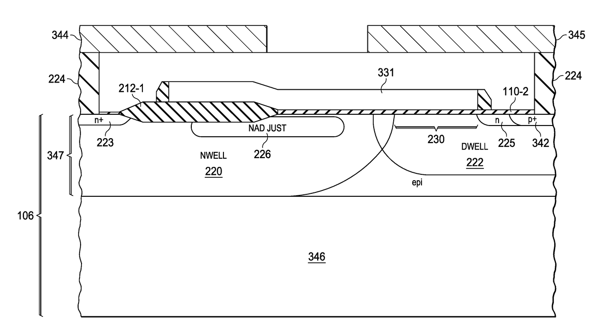
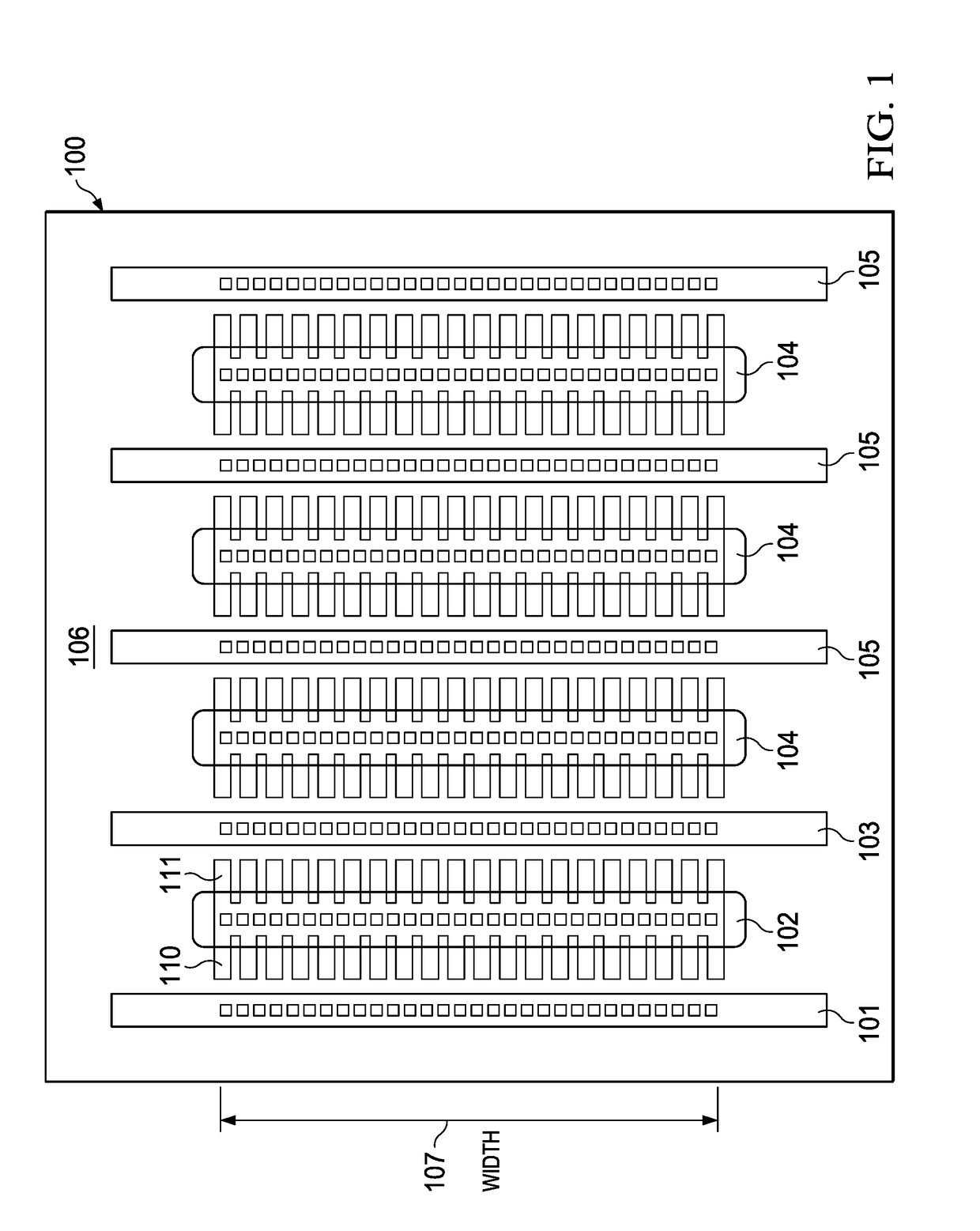
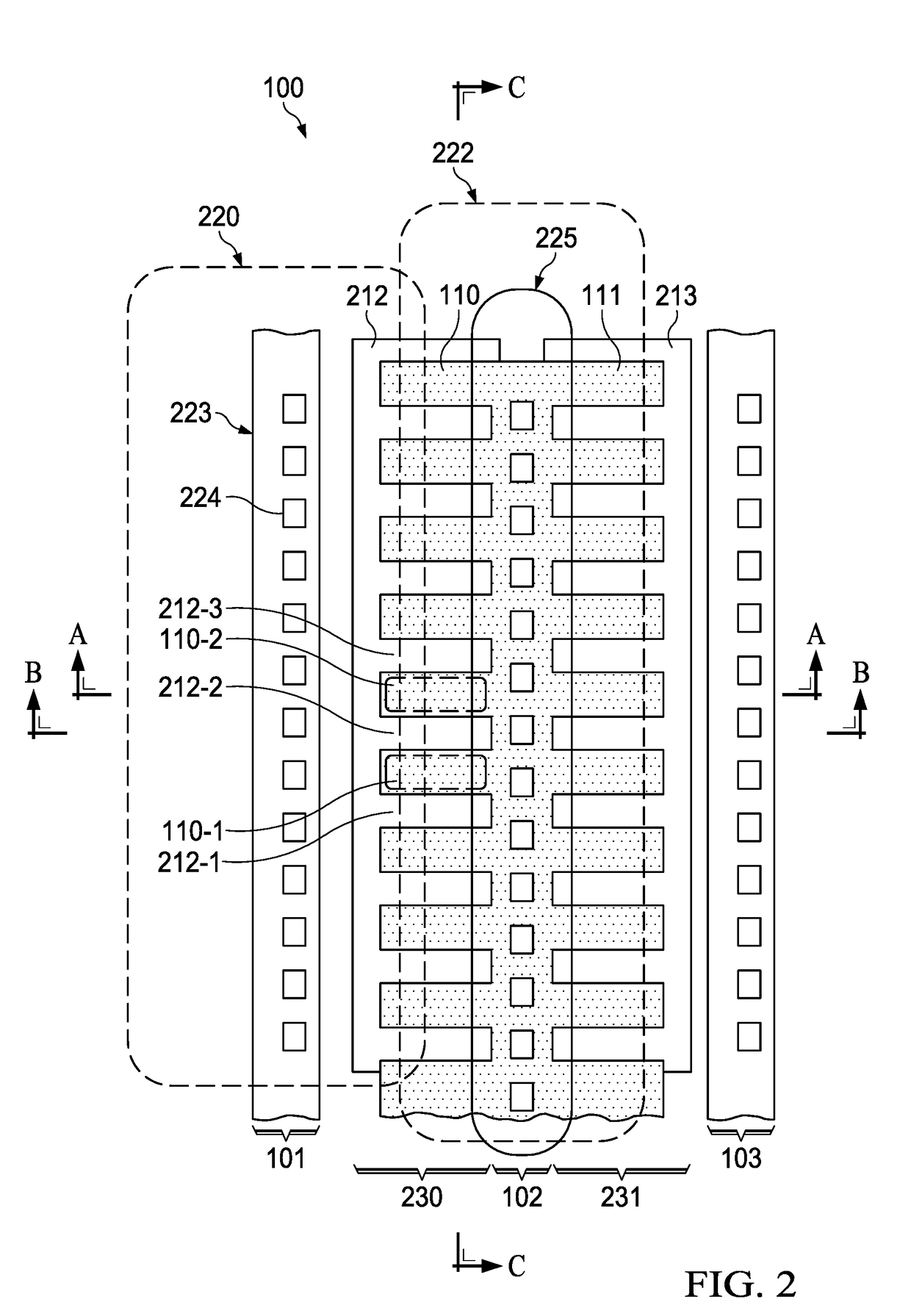
[0014]In an LDMOS transistor, a lightly doped lateral diffused drain region is constructed between the heavily doped drain contact and the transistor channel region. As the name implies, a lateral current is created between drain and source. A depletion region forms in this lightly doped lateral diffused region resulting in a voltage drop between the drain contact and the transistor gate. With proper design, sufficient voltage may be dropped between the drain contact and the gate dielectric to allow a low gate voltage transistor to be used as a switch for a high voltage load, for example.

[0015]A ...


PUM


Abstract

A power transistor is provided with at least one transistor finger that lies within a semiconductor material. The gate oxide is segmented into a set of segments with thick field oxide between each segment in order to reduce gate capacitance and thereby improve a resistance times gate charge figure of merit.

Description

CROSS REFERENCE TO RELATED APPLICATIONS[0001]Under 35 U.S.C. § 120, this continuation application claims benefits of and priority to U.S. patent application Ser. No. 15 / 385,709 (TI-76809), filed on Dec. 20, 2016, the entirety of which are hereby incorporated herein by reference.FIELD OF THE DISCLOSURE[0002]This disclosure relates to power transistors, and in particular to laterally diffused metal oxide semiconductor devices.BACKGROUND OF THE DISCLOSURE[0003]Power transistors are found in many common electronic devices, including power supplies, voltage converters, integrated circuits, and low-voltage motor controllers. Laterally diffused metal oxide semiconductor (LDMOS) transistors are one type of power transistor and are also used in microwave and radio frequency (RF) power amplifiers, for example. These transistors are often fabricated on p / p+ silicon epitaxial layers.[0004]LDMOS transistors are MOS transistors that also have a drain drift region. The drain drift region, which to...

Claims


Application Information

Patent Timeline
Patent Type & Authority Applications(United States)
IPC IPC(8): H01L29/78H01L29/66H01L29/40H01L29/423H01L29/06
CPCH01L29/66681H01L29/408H01L29/7816H01L29/42368H01L29/0696H01L29/42364H01L29/0878H01L29/66689H01L29/1095
Inventor PENDHARKAR, SAMEERCHUANG, MING-YEH
Owner TEXAS INSTR INC
Why Eureka
Try Eureka