High resolution demultiplexer driver circuit

Active Publication Date: 2018-06-28
WUHAN CHINA STAR OPTOELECTRONICS TECH CO LTD
View PDF1 Cites 14 Cited by
  • Summary
  • Abstract
  • Description
  • Claims
  • Application Information

AI Technical Summary

Benefits of technology

[0018]Compared to the known techniques, the present invention provides the following advantages: the present invention provides a high resolution demux driver circuit, wherein the data signal does not change voltage

Problems solved by technology

As the recent development of high pixel per inch (PPI) panel, more and more panels of higher resolution consume more power due to heavier load and higher

Method used


Image

  • High resolution demultiplexer driver circuit
  • High resolution demultiplexer driver circuit
  • High resolution demultiplexer driver circuit

Examples


Embodiment Construction

[0028]To further explain the technical means and effect of the present invention, the following refers to embodiments and drawings for detailed description.

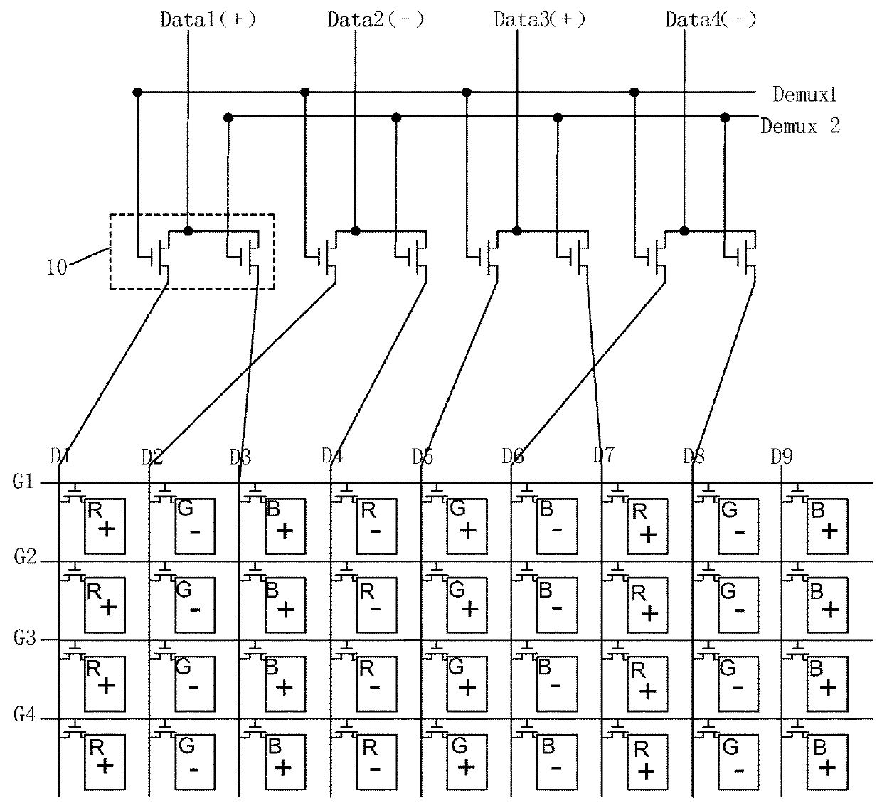
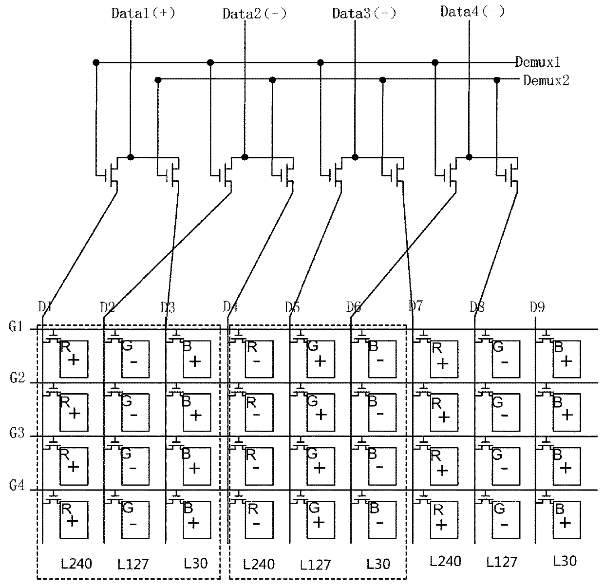
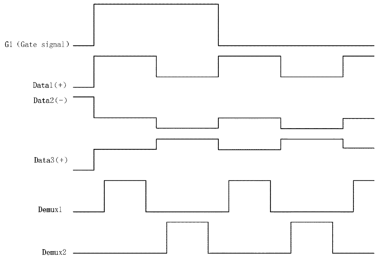
[0029]Refer to FIG. 4. The preferred embodiment of high resolution demultiplexer (demux) driver circuit provided by the present invention comprises: a plurality of scan lines G1, G2, . . . , connected respectively to sub-pixels of a corresponding column, a plurality of data lines D1, D2, . . . , connected respectively to sub-pixels of a corresponding row, and a plurality of multiplexer (mux) modules 20; each mux module 20 comprising two thin film transistors (TFTs), with the gates connected respectively to a first shunt control signal Demux1 and a second shunt control signal Demux2, the sources connected to a same data signal, and the drains connected respectively to a data line near the two same color sub-pixel row to achieve using the same data signal to perform 1-to-2 demultiplexing; the drains of the mux modules 20 at the fir...


PUM


Abstract

The invention provides a high resolution demultiplexer (demux) driver circuit, comprising: a plurality of scan lines connected respectively to sub-pixels of corresponding column, a plurality of data lines connected respectively to sub-pixels of corresponding row, and a plurality of multiplexer (mux) modules; each mux module comprising two thin film transistors, with gates connected respectively to first and second shunt control signals, sources connected to same data signal, and drains connected respectively to data line near the two same color sub-pixel row; controlling the polarity of each data signal to control each sub-pixel row except the first and last rows to display in horizontal direction following the polarity distribution of alternating positive-positive and negative-negative. The invention does not need to change the data signal voltage in a power-saving mode, and achieves high power-saving efficiency. The number of control signals and the frequency controlling control signals are reduced for further power-saving.

Description

BACKGROUND OF THE INVENTION1. Field of the Invention[0001]The present invention relates to the field of display, and in particular to a high resolution demultiplexer (demux) driver circuit.2. The Related Arts[0002]The panel display devices, such as, liquid crystal display (LCD) and organic light-emitting diode (OLED) display, comprise a plurality of pixels arranged in an array. Each pixel usually comprises three sub-pixels of red, green and blue respectively. Each sub-pixel is controlled by a gate line and a data line. The gate line is to control the sub-pixel for conduction state, i.e., ON and OFF. The data line is to apply different data voltages to the sub-pixel so that the sub-pixel displays different grayscale to achieve full color display.[0003]As the recent development of high pixel per inch (PPI) panel, more and more panels of higher resolution consume more power due to heavier load and higher frequency. One of the major power consumption comes from the design of the demulti...

Claims


Application Information

Patent Timeline
IPC IPC(8): G09G3/36G09G3/3225
CPCG09G3/3614G09G3/3648G09G3/3225G09G2310/0297G09G2330/021G09G3/3688G09G2340/0407G09G3/36
Inventor LIN, JIANHONG
Owner WUHAN CHINA STAR OPTOELECTRONICS TECH CO LTD
Why Eureka
Try Eureka