Eureka AIR delivers breakthrough ideas for toughest innovation challenges, trusted by R&D personnel around the world.

Method and system for vertical power devices

Active Publication Date: 2018-06-28
QROMIS INC
View PDF0 Cites 1 Cited by
  • Summary
  • Abstract
  • Description
  • Claims
  • Application Information

AI Technical Summary

Benefits of technology

The present invention provides methods for forming semiconductor devices using an engineered substrate. The engineered substrate includes a polycrystalline ceramic core, a barrier layer, a bonding layer, and a substantially single crystalline silicon layer. The methods include forming a Schottky diode and a Schottky contact on the substrate, as well as a power transistor with a drain contact. The power transistor has a structure that includes a trench and a channel region. The methods also include forming an epitaxial aluminum gallium nitride layer and a gate dielectric layer on the substrate. The technical effects of the invention include improved performance and reliability of semiconductor devices that use the engineered substrate.

Problems solved by technology

Due to the heteroepitaxial growth process, the epitaxially grown material can exhibit a variety of adverse effects, including reduced uniformity and reductions in metrics associated with the electronic / optical properties of the epitaxial layers.

Method used


Image

  • Method and system for vertical power devices
  • Method and system for vertical power devices
  • Method and system for vertical power devices

Examples


Embodiment Construction

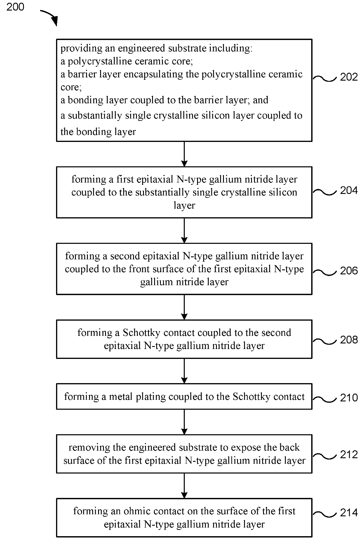
[0017]The present invention relates generally to Schottky diodes and power transistors formed on engineered substrates. More specifically, the present invention relates to methods and systems suitable for fabricating vertical Schottky diodes and vertical power transistors using epitaxial growth processes. Merely by way of example, the invention has been applied to a method and system for fabricating vertical Schottky diodes and vertical power transistors on a substrate by epitaxial growth, wherein the substrate is characterized by a coefficient of thermal expansion (CTE) that is substantially matched to epitaxial layers that form the vertical Schottky diodes and vertical power transistors. The methods and techniques can be applied to a variety of semiconductor processing operations.

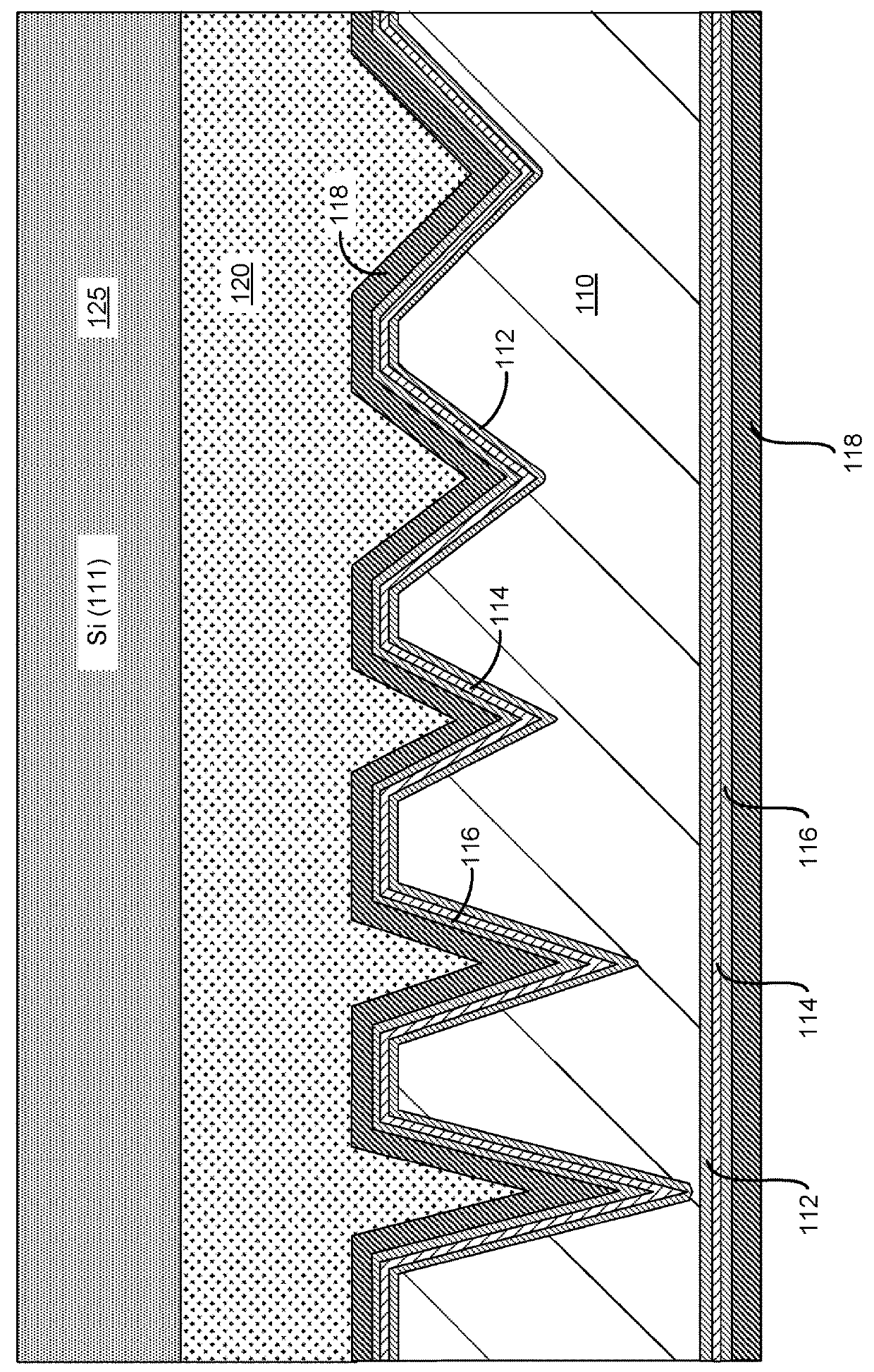
[0018]FIG. 1 is a simplified schematic diagram illustrating an engineered substrate structure according to some embodiments of the present invention. As illustrated in FIG. 1, the engineered substrate str...


PUM


Abstract

A method of forming a semiconductor device includes providing an engineered substrate. The engineered substrate includes a polycrystalline ceramic core, a barrier layer encapsulating the polycrystalline ceramic core, a bonding layer coupled to the barrier layer, and a substantially single crystalline silicon layer coupled to the bonding layer. The method further includes forming a Schottky diode coupled to the engineered substrate. The Schottky diode has a top surface and a bottom surface. the bottom surface is coupled to the substantially single crystalline silicon layer. The method further includes forming a Schottky contact coupled to the top surface of the Schottky diode, forming a metal plating coupled to the Schottky contact, removing the engineered substrate to expose the bottom surface of the Schottky diode, and forming an ohmic contact on the bottom surface of the Schottky diode.

Description

CROSS-REFERENCES TO RELATED APPLICATIONS[0001]This application claims the benefit of U.S. Provisional Patent Application No. 62 / 439,860, filed on Dec. 28, 2016, the disclosure of which is incorporated by reference in its entirety.BACKGROUND OF THE INVENTION[0002]Gallium nitride based power devices are typically epitaxially grown on sapphire substrates. The growth of gallium nitride based power devices on a sapphire substrate is a heteroepitaxial growth process since the substrate and the epitaxial layers are composed of different materials. Due to the heteroepitaxial growth process, the epitaxially grown material can exhibit a variety of adverse effects, including reduced uniformity and reductions in metrics associated with the electronic / optical properties of the epitaxial layers. Accordingly, there is a need in the art for improved methods and systems related to epitaxial growth processes and substrate structures.SUMMARY OF THE INVENTION[0003]According to an embodiment of the pres...

Claims


Application Information

Patent Timeline
IPC IPC(8): H01L21/02H01L21/683H01L29/66H01L21/78
CPCH01L21/02505H01L21/6831H01L21/0242H01L21/02488H01L21/02516H01L21/0245H01L21/0254H01L29/66212H01L21/02389H01L21/7806H01L29/66522H01L29/66712H01L21/02378H01L21/0243H01L21/02002H01L29/66462H01L29/7788H01L29/872H01L29/2003H01L29/41766H01L29/0603H01L29/0646
Inventor ODNOBLYUDOV, VLADIMIRRISBUD, DILIPAKTAS, OZGUR
Owner QROMIS INC
Why Eureka
Eureka Blog
Learn More