Packaged resonator with polymeric air cavity package

a resonator and air cavity technology, applied in the direction of impedence networks, electric devices, etc., can solve the problems of filter technology, high resistive materials, and a high barrier to the overall system miniaturization,

Active Publication Date: 2018-06-28
AVAGO TECH INT SALES PTE LTD
View PDF8 Cites 40 Cited by
  • Summary
  • Abstract
  • Description
  • Claims
  • Application Information

AI Technical Summary

Problems solved by technology

Many known filter technologies present a barrier to overall system miniaturization.
These induced currents themselves generate electromagnetic radiation that can interfere with the desired electrical signals of the resonator and can degrade the performance of devices (e.g., filters) that incorporate the resonator.
While some improvements are realized using undoped, highly resistive materials for the substrate, third order IMD products (IMD3) remain problematic especially as higher power transmission and reception, and reduced channel spacing, drives the communications industry.
Parasitic contributions from the microcap lid wafer / microcap lid degrade linear performance characteristics of the packaged FBAR product.
The gold thermocompression bond is expensive.
At least in part to due to this expense, the size of the area in which the posts are attached to the substrate is limited, and the gold thermocompression bond is used only around a perimeter of the posts.
Additionally, the gold thermocompression bond is used at high-pressure / high-temperature which poses a potential obstacle to scaling FBARs to wafers larger than, for example, 200 millimeters.
In the silicon microcap device, these air gaps require difficult singulation technologies that may often result in perimeter chip-out which must be screened by testing in the final product.
In known devices, these induced currents can contribute to intermodulation distortion (IMD) products.
These structures, which include carriers, are susceptible to induced currents from electromagnetic radiation in their vicinity.
In the silicon microcap device, these air gaps require difficult singulation technologies that frequently result in perimeter chip-out, which must be screened by testing in the final product.

Method used


Image

  • Packaged resonator with polymeric air cavity package
  • Packaged resonator with polymeric air cavity package
  • Packaged resonator with polymeric air cavity package

Examples


Embodiment Construction

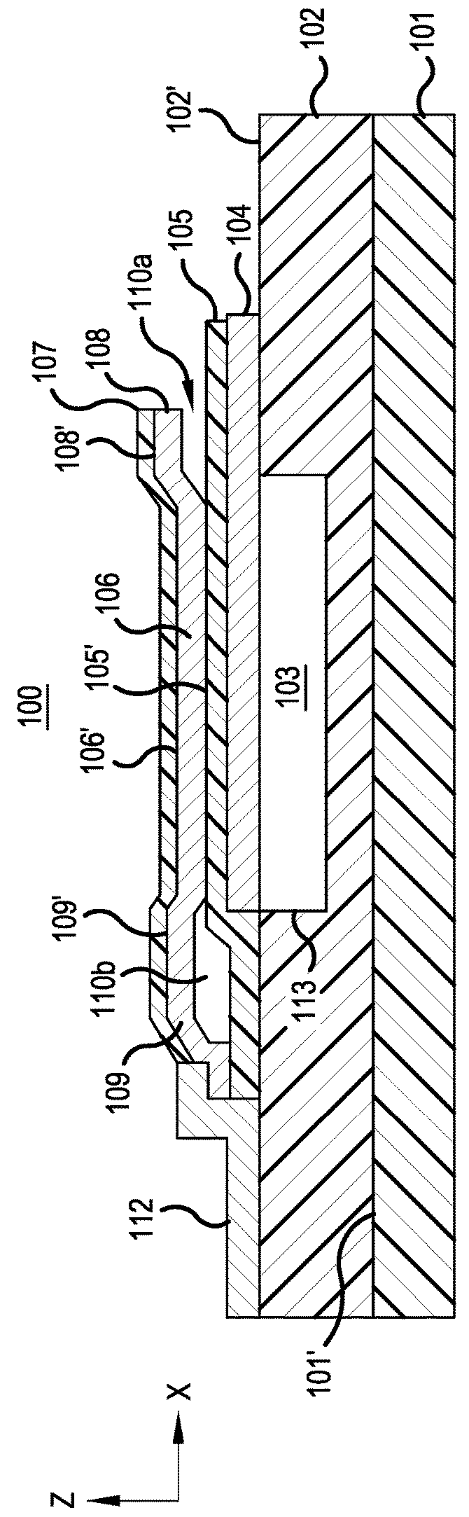
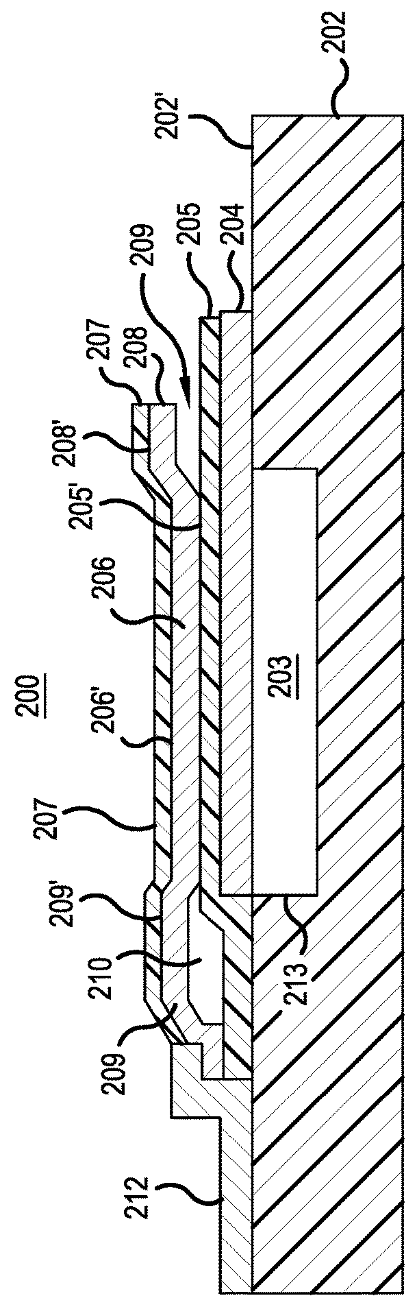
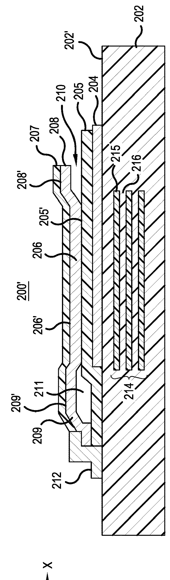
[0029]In the following detailed description, for purposes of explanation and not limitation, example embodiments disclosing specific details are set forth in order to provide a thorough understanding of the present teachings. However, it will be apparent to one having ordinary skill in the art having the benefit of the present disclosure that other embodiments according to the present teachings that depart from the specific details disclosed herein remain within the scope of the appended claims. Moreover, descriptions of well-known apparatuses and methods may be omitted so as to not obscure the description of the example embodiments. Such methods and apparatuses are clearly within the scope of the present teachings.

[0030]The terminology used herein is for purposes of describing particular embodiments only, and is not intended to be limiting. The defined terms are in addition to the technical, scientific, or ordinary meanings of the defined terms as commonly understood and accepted i...


PUM


Abstract

A packaged resonator includes a substrate, an acoustic stack, a first polymer layer and a second polymer layer. The acoustic stack is disposed over the substrate. The first polymer layer is disposed over the substrate surrounding the acoustic stack. The first polymer layer also provides a first air gap above the acoustic stack. The second polymer layer is disposed over the acoustic stack and above the first air gap.

Description

CROSS-REFERENCE TO RELATED APPLICATIONS[0001]The present application is a continuation-in-part application under 37 C.F.R. § 1.53(b) of commonly owned U.S. patent application Ser. No. 15 / 390,430 to Chris Feng, et al., entitled “Bulk BAW Resonator Having Electrically Insulating Substrate,” and filed on Dec. 23, 2016. The entire disclosure of U.S. patent application Ser. No. 15 / 390,430 is specifically incorporated herein by reference, and for all purposes.BACKGROUND[0002]Electrical resonators are used in many electronic applications. For example, acoustic resonators are an enabling technology for radio frequency (RF) mobile communications. In many wireless communications devices, RF as well as microwave frequency resonators are used as filters to improve reception and transmission of signals. Acoustic resonators act as low loss and high fidelity filters for the many frequency bands upon which modern mobile communications are based. Filters typically include inductors and capacitors, a...

Claims


Application Information

Patent Timeline
Patent Type & Authority Applications(United States)
IPC IPC(8): H03H9/17
CPCH03H9/171H03H3/02H03H9/02118H03H9/1014H03H9/173H03H2003/021
Inventor PATIL, VIKRAMCHOY, JOHN
Owner AVAGO TECH INT SALES PTE LTD
Why Eureka
Try Eureka