Supercharge Your Innovation With Domain-Expert AI Agents!

Electronic device including a tunnel layer

a tunnel layer and electromechanical technology, applied in the direction of basic electric elements, semiconductor devices, electrical equipment, etc., can solve the problems of increasing the operating voltage and thermal energy consumption, reducing the characteristic of the device, and difficult to use the metal-silicon junction, so as to reduce the contact resistance of a portion

Active Publication Date: 2018-07-05
SAMSUNG ELECTRONICS CO LTD
View PDF7 Cites 3 Cited by
  • Summary
  • Abstract
  • Description
  • Claims
  • Application Information

AI Technical Summary

Benefits of technology

This approach effectively lowers the contact resistance and eliminates Fermi-level pinning, enabling a low-resistance metal-semiconductor junction, reducing the need for high doping densities and preventing short channel effects, thus improving device performance and miniaturization.

Problems solved by technology

In this case, a contact resistance between the metal and the silicon increases, thereby resulting in an increase in an operating voltage and consumption as thermal energy, and thus it is difficult to use the metal-silicon junction.
In addition, when a device size decreases, doping portions of a source and a drain meet each other, thereby resulting in a short channel effect such that a channel is not normally formed and causing a decrease in a device characteristic.
However, it is typically difficult to uniformly generate a thin oxide layer, and if the thickness of the thin oxide layer is thick to a certain level, a contact resistance increases.

Method used


Image

  • Electronic device including a tunnel layer
  • Electronic device including a tunnel layer
  • Electronic device including a tunnel layer

Examples


Embodiment Construction

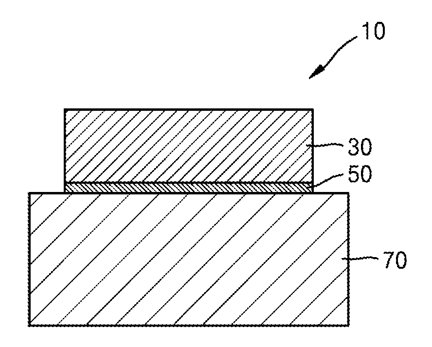
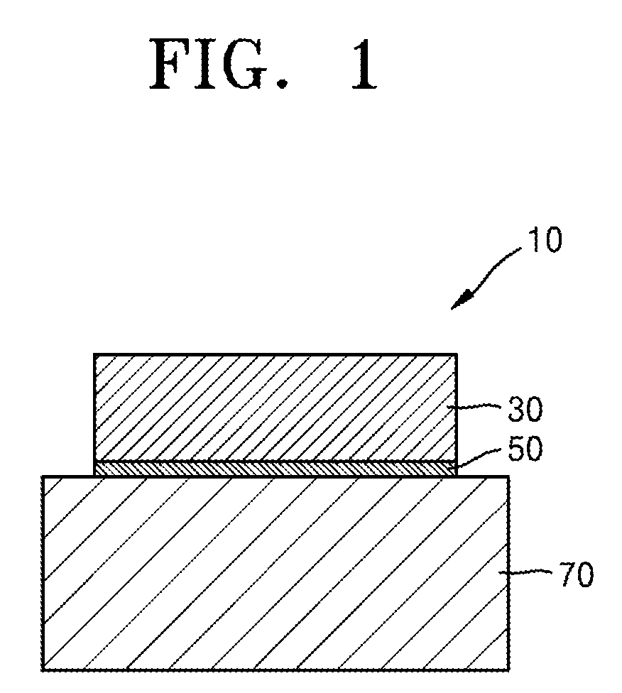
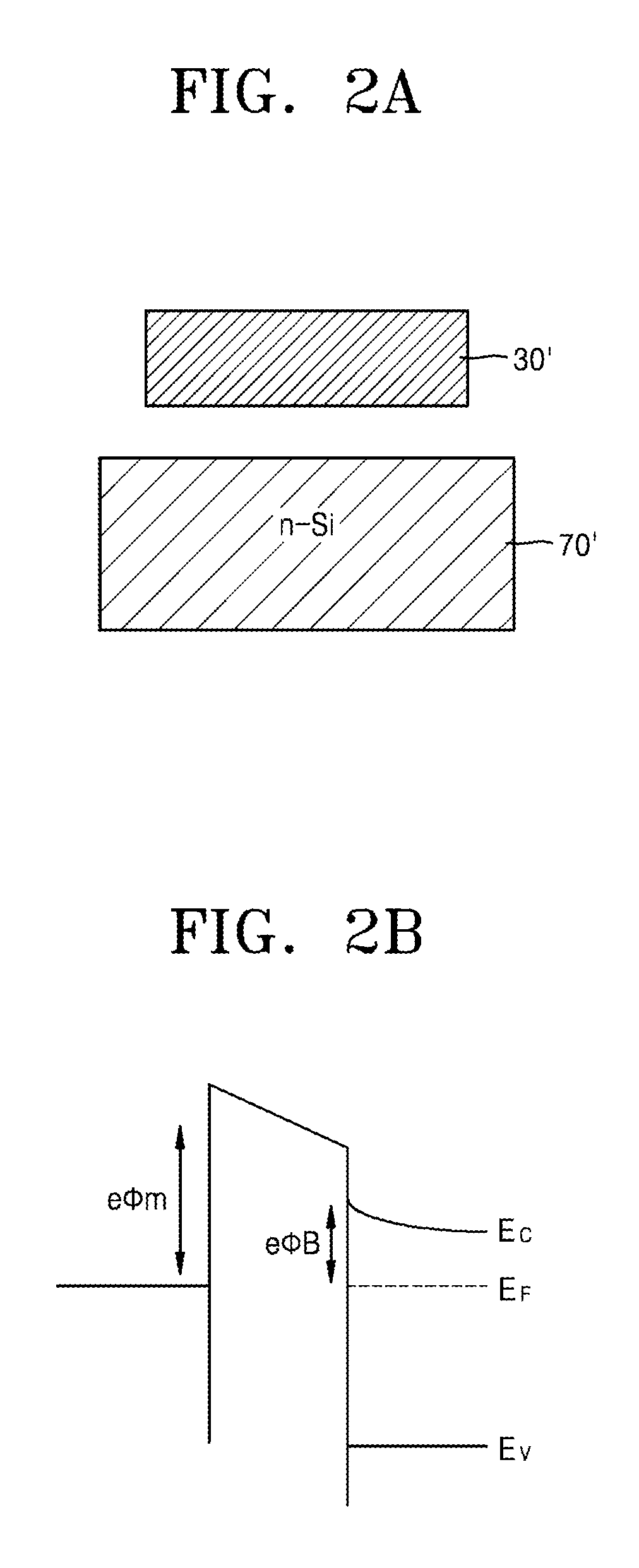
[0036]An electronic device and a transistor, of which an energy barrier between a semiconductor substrate and a metal is reduced using graphene, according to example embodiments will now be described in detail with reference to the accompanying drawings. In the drawings, like reference numerals refer to like elements throughout, and the sizes, the thicknesses, and the like of components in the drawings may be exaggerated for clarity and convenience of description. In addition, when it is described that a certain component is “above,”“on the upper part of,” or “on” another component, the certain component may be directly above another component, or a third component may be interposed therebetween. In this regard, the example embodiments may have different forms and should not be construed as being limited to the descriptions set forth herein. Accordingly, the example embodiments are merely described below, by referring to the figures, to explain example embodiments of the present des...


PUM


Abstract

An electronic device includes a semiconductor layer, a tunneling layer formed of a material including a two-dimensional (2D) material so as to directly contact a certain region of the semiconductor layer, and a metal layer formed on the tunneling layer.

Description

RELATED APPLICATIONS[0001]This is a divisional application of U.S. application Ser. No. 14 / 528,338, filed on Oct. 30, 2014, which claims priority from Korean Patent Application No. 10-2013-0147524, filed on Nov. 29, 2013, in the Korean Intellectual Property Office, the disclosure of which is incorporated herein in its entirety by reference.BACKGROUND1. Field[0002]Example embodiments relate to electronic devices, and more particularly, to electronic devices configured to reduce a contact resistance of a portion at which a metal and a semiconductor meet.2. Description of the Related Art[0003]When a metal is junctioned, adjoined or coupled to a semiconductor, such as silicon, a Schottky energy barrier is generated due to a work function difference between the two materials and a Fermi-level pinning phenomenon of the work function of the metal on the surface of the silicon. In this case, a contact resistance between the metal and the silicon increases, thereby resulting in an increase i...

Claims


Application Information

Patent Timeline
Patent Type & Authority Applications(United States)
IPC IPC(8): H01L29/66H01L29/78H01L29/45
CPCH01L29/78H01L29/456H01L29/66977H01L29/49H01L29/51H01L29/772
Inventor BYUN, KYUNGEUNKYOUNG, JISOOPARK, SEONGJUNSHIN, HYEONJINSONG, HYUNJAELEE, JAEHO
Owner SAMSUNG ELECTRONICS CO LTD
Features
  • R&D
  • Intellectual Property
  • Life Sciences
  • Materials
  • Tech Scout
  • Unparalleled Data Quality
  • Higher Quality Content
  • 60% Fewer Hallucinations
Learn More