Solid-state imaging device

Active Publication Date: 2018-07-12
PANASONIC INTELLECTUAL PROPERTY MANAGEMENT CO LTD
View PDF0 Cites 4 Cited by
  • Summary
  • Abstract
  • Description
  • Claims
  • Application Information

AI Technical Summary

Benefits of technology

[0009]According to the present disclosure, a solid-state imaging device can be realized in which an avalanche photodiode and a pixel circuit a

Problems solved by technology

However, light cannot be detected in a region in which a pixel circuit is disposed, and decline in the sensitivity due to a reduced aperture ratio has been a problem.
However, since it is difficult to achieve miniaturization with this technique, there is a problem that it is difficult to obtain a high resolution.
However, in this structure, signal charge e

Method used


Image

  • Solid-state imaging device
  • Solid-state imaging device
  • Solid-state imaging device

Examples


Example

Embodiment 1

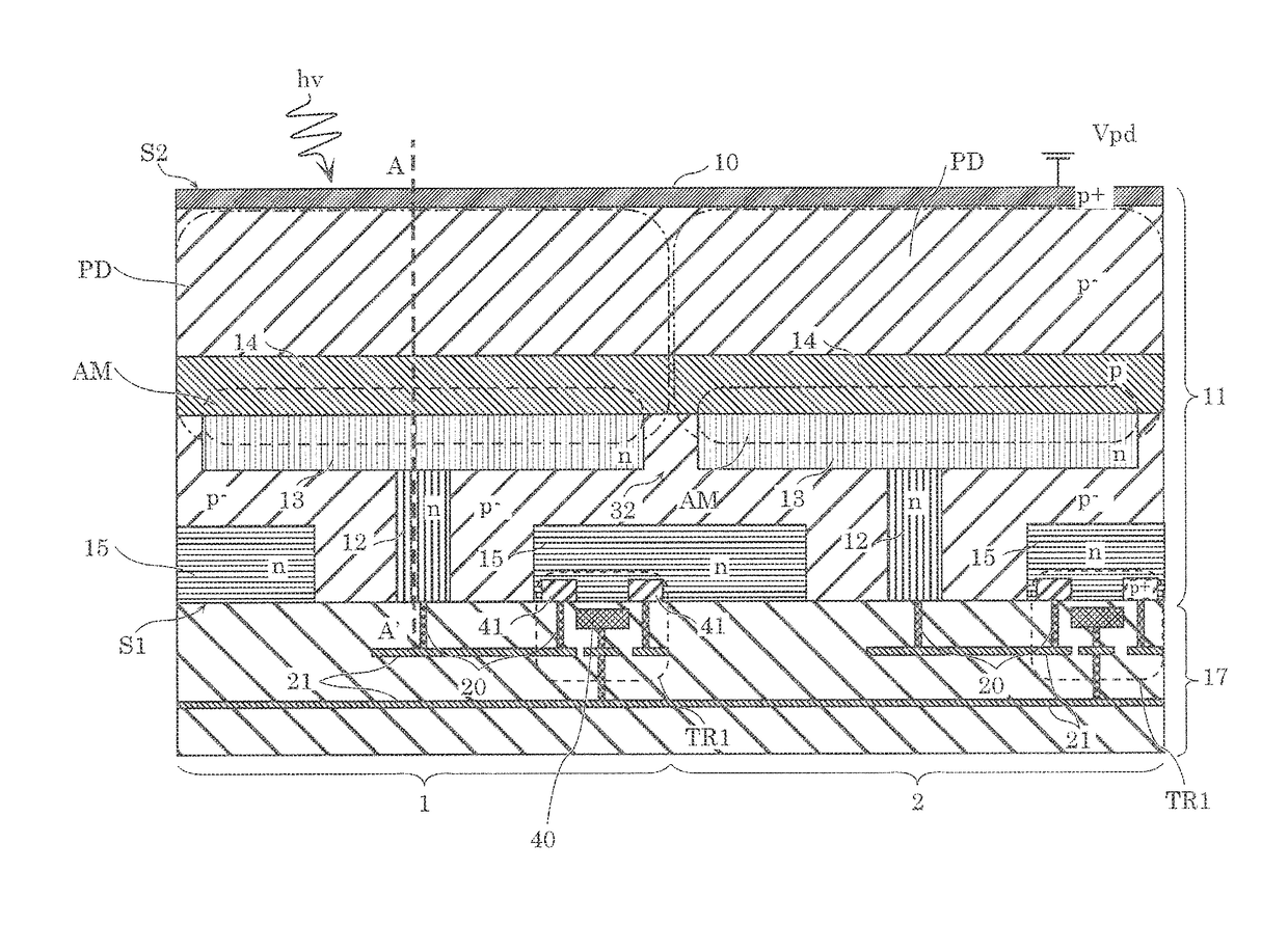
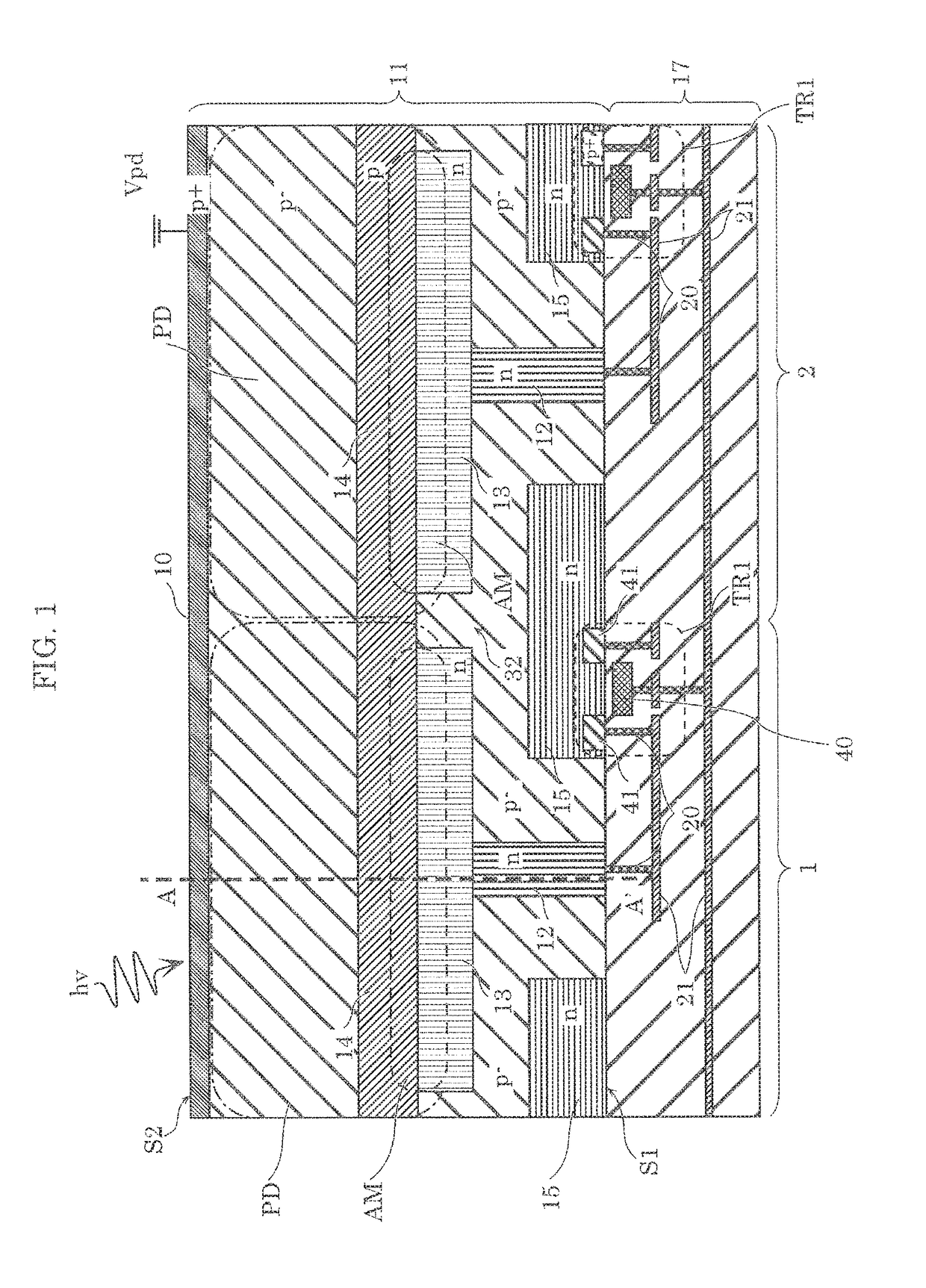
[0029]First, a structure of a solid-state imaging device according to Embodiment 1 will be described with reference to FIG. 1 and FIG. 2. Note that, in the present specification, “planar view” indicates a view in the direction normal to first principal surface S1 and second principal surface S2 shown in FIG. 1.

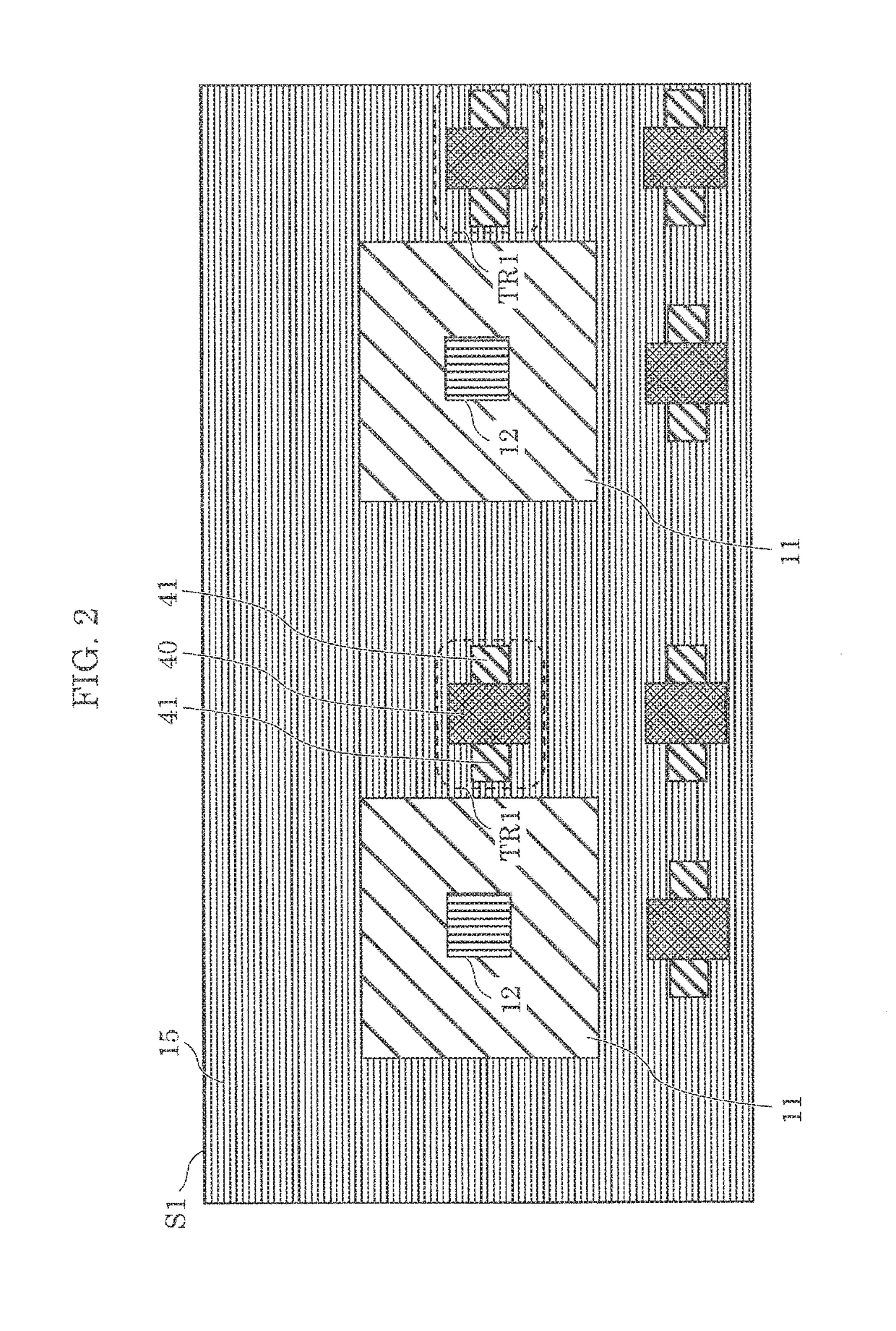
[0030]FIG. 1 is a cross-sectional view of a pixel array (here, pixel 1 and pixel 2) included in a solid-state imaging device in the case where transistor TR1 is a P channel transistor. FIG. 2 is a plan view of first principal surface S1 of FIG. 1, which is seen in the direction of second principal surface S2. FIG. 2 also illustrates gate electrodes 40 of transistors TR1 for better understanding of the positional relationships. FIG. 3 is a graph showing a potential gradient at A-A′ line in FIG. 1, when fixed potential Vpd is applied to P+ type semiconductor region 10. Note that, when simply a “transistor” is referred to in the present embodiment, this means that the...

Example

Embodiment 2

[0052]Next, a structure of a solid-state imaging device according to Embodiment 2 is described with reference to FIG. 6. FIG. 6 is a cross-sectional view of the solid-state imaging device according to Embodiment 2 in the case where transistor TR1 is an N channel transistor. FIG. 7 is a plan view of first principal surface S1 in FIG. 6, which is viewed in the direction of second principal surface S2. FIG. 7 also illustrates gate electrodes 40 of the transistors for better understanding of the positional relationships.

[0053]In this case, it is necessary to form P type well 22 in each N type well 15. P type well 22 is another example of the first well region for forming transistor TR1. Even at the time of the avalanche multiplication driving, the potential of P type well 22 should be fixed to determine the voltage for driving the N channel transistor TR1. In order to achieve this, since P+ type semiconductor region 10 to which fixed potential Vpd is applied needs to be elec...

Example

Embodiment 3

[0060]FIG. 8 is a cross-sectional view of a solid-state imaging device according to Embodiment 3. FIG. 9 is a plan view of first principal surface S1 in FIG. 8, which is viewed in the direction of second principal surface S2. FIG. 9 also illustrates gate electrodes 40 of the transistors for better understanding of the positional relationships. FIG. 10 is a plan view when the cross-section taken along line A-A′ of FIG. 8 is viewed in the direction of second principal surface S2. FIG. 11 is a plan view when the cross-section taken along line B-B′ of FIG. 8 is viewed in the direction of second principal surface S2. FIG. 12 is a graph showing the potential gradient at C-C′ line of FIG. 8 when fixed potential Vpd is applied to P+ type semiconductor region 10. In FIG. 8 to FIG. 12, elements that are essentially the same as Embodiment 1 share like reference signs. Moreover, the following description will focus on the points different from Embodiment 1.

[0061]Between N type semic...


PUM


Abstract

A solid-state imaging device includes a substrate of P type and a wiring layer. The substrate includes: a first semiconductor region disposed on a first principle surface and extending in a direction from the first principal surface toward the second principal surface; a second semiconductor region disposed between the second principal surface and the first semiconductor region and connected to the first semiconductor region; a P type semiconductor region disposed between the second principal surface and the second semiconductor regions of two pixels; and a pixel isolation region disposed inside the substrate, between the first semiconductor regions of the two pixels. The second semiconductor region and the P type semiconductor region form an avalanche multiplication region.

Description

CROSS REFERENCE TO RELATED APPLICATIONS[0001]This application is a U.S. continuation application of PCT International[0002]Patent Application Number PCT / JP2016 / 004058 filed on Sep. 6, 2016, claiming the benefit of priority of U.S. Provisional Patent Application No. 62 / 216238 filed on Sep. 9, 2015 and U.S. Provisional Patent Application No. 62 / 275998 filed on Jan. 7, 2016, the entire contents of which are hereby incorporated by reference.BACKGROUND1. Technical Field[0003]The present disclosure relates to a solid-state imaging device, and particularly relates to a solid-state imaging device which detects weak light.2. Description of the Related Art[0004]In recent years, high sensitivity cameras are used in various fields such as medicine, biotechnology, chemistry, surveillance, in-vehicle, radiation detection, and so on. Avalanche photodiodes (hereinafter, also referred to as APDs) have been used as one of the ways to improve the sensitivity of cameras. APDs are photodiiodes having li...

Claims


Application Information

Patent Timeline
IPC IPC(8): H01L27/146H01L31/107H04N5/374
CPCH01L27/1463H01L31/107H04N5/374H04N5/378H01L27/14612H01L27/1464H01L27/14643H04N25/621H04N25/70H04N25/76H01L31/1075H04N25/75H01L31/00
Inventor SAKATA, YUSUKEUSUDA, MANABUMORI, MITSUYOSHIKATO, YOSHIHISA
Owner PANASONIC INTELLECTUAL PROPERTY MANAGEMENT CO LTD
Why Eureka
Try Eureka