Unlock instant, AI-driven research and patent intelligence for your innovation.

Semiconductor memory device and reading method for the same

a data reading and memory device technology, applied in static storage, digital storage, instruments, etc., can solve the problems of high operation frequency of serial clock signal sclk, inability to read data correctly, and large latency, so as to achieve the effect of correct read-out data

Active Publication Date: 2018-07-19
WINBOND ELECTRONICS CORP
View PDF2 Cites 2 Cited by
  • Summary
  • Abstract
  • Description
  • Claims
  • Application Information

AI Technical Summary

Benefits of technology

The present invention allows for verification of the correctness of read-out data through a verification circuit. Additionally, when the verification circuit identifies an incorrect read-out data, the m-bit data can be selected from the sensed n-bit data by controlling the timing of an activation signal. This results in output of correct read-out data even at high operation frequencies.

Problems solved by technology

When the operation frequency of the serial clock signal SCLK becomes high, in the read operation, the read-out data cannot be accurately fetched to the input / output circuit 60 by a pipeline in response to the internal clock signal PSCCLK synchronized with the serial clock signal SCLK, and thus incorrect data may be output.
FIG. 3 is a schematic view showing a problem when the operation frequency of the serial clock signal SCLK becomes high.
Thus, the latency becomes very large.

Method used


Image

  • Semiconductor memory device and reading method for the same
  • Semiconductor memory device and reading method for the same
  • Semiconductor memory device and reading method for the same

Examples


Embodiment Construction

[0032]Hereinafter, embodiments of the present invention will be described in detail with reference to the drawings. In a preferred embodiment, the read-out data verification circuit of the present invention is configured in a semiconductor device (for example, a NAND flash memory or other semiconductor memory) having a serial interface. In another preferred embodiment, the read-out data verification circuit of the present invention can be externally connected to a semiconductor device having a serial interface. The serial interface comprises, for example, a terminal for inputting a serial clock SCLK, terminals for inputting / outputting data, commands, addresses and the like, a terminal for performing a chip selection, and the like.

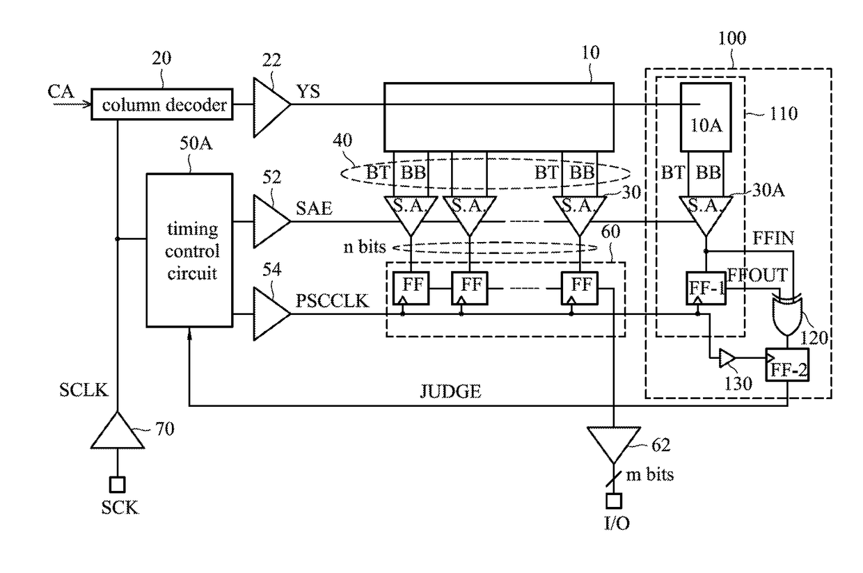
[0033]Next, embodiments of the present invention will be described. FIG. 4 an exemplary embodiment of a verification circuit 100 configured in a flash memory, and the same reference numerals are attached to the same components as those shown in FIG. 1.

[0034...


PUM


Abstract

A semiconductor memory device is provided. The semiconductor memory device includes a column selection circuit, a sensing circuit, an output circuit, and a verification circuit. The column selection circuit selects n-bit data from data read from a memory cell array according to a column selection signal and outputs the selected n-bit data to an n-bit data bus. The sensing circuit senses the n-bit data on the data bus in response to an activation signal. The output circuit selects m-bit data from the n-bit data sensed by the sensing circuit in response to an internal clock signal synchronized with a serial clock signal applied from outside and outputs the selected m-bit data from output terminals. The verification circuit compares the data sensed by the sensing circuit with the data output by the output circuit to verifying the correctness of read-out data.

Description

CROSS REFERENCE TO RELATED APPLICATIONS[0001]This Application claims priority of Japan Patent Application No. JP2017-003785, filed on Jan. 13, 2017, the entirety of which is incorporated by reference herein.BACKGROUND OF THE INVENTIONField of the Invention[0002]The invention relates to a data reading method for a semiconductor memory device, and more particularly to a method for verifying data read from a NAND flash memory with a serial interface function.Description of the Related Art[0003]In a NAND flash memory, data is read and programmed in a unit of one page, and the page data is stored in a page buffer. The flash memory disclosed in Patent Document 1 has a first mode in which the data stored is transmitted in a first bit-width and a second mode in which the data is transmitted in a second bit-width, and these modes correspond to several operation modes.[0004][Patent Document 1]: Japanese Patent Publication No. 2012-253591.[0005]A NAND flash memory are equipped with a serial in...

Claims


Application Information

Patent Timeline
IPC IPC(8): G11C7/12G11C16/32G11C7/06G11C7/10
CPCG11C7/12G11C7/109G11C16/32G11C7/06G11C2216/14G11C16/26G11C16/0483G11C7/1021G11C7/103G11C16/3422
Inventor KOJIMA, HIDEMITSU
Owner WINBOND ELECTRONICS CORP