Solid-state imaging device, and method of manufacturing solid-state imaging device

Active Publication Date: 2018-09-27
SONY SEMICON SOLUTIONS CORP
View PDF13 Cites 5 Cited by
  • Summary
  • Abstract
  • Description
  • Claims
  • Application Information

AI Technical Summary

Benefits of technology

[0067]In the solid-state imaging device 1 as described above, in a case where light enters the organic photoelectric conversion film 14 through the first sealing film 16 and the second electrode 15, a portion of the entering light (e.g., green light) is selectively absorbed. As a result, in the organic photoelectric conversion film 14, electron-hole pairs are generated (photoelectric conversion is performed), and one of the electrons and the holes are collected, for example, on the first electrodes 13 side and are accumulated in the charge accumulation layers 112 in the semiconductor substrate 11. The electric charges accumulated in the charge accumulation layers 112 are read out as the electric signal to the peripheral circuits through the transfer transistor Tr. In contrast, light having passed through the organic photoelectric conversion film 14 (e.g., blue light and red light) is sequentially absorbed by the photoelectric conversion devices 110B and 110R in the semiconductor substrate 11 and is photoelectrically converted, and is read out as an electric signal for each color.
[0068]In this case, in the solid-state imaging device 1 having the above-described organic photoelectric conversion film 14, the first sealing film 16 that covers the plurality of pixels P is formed in order to prevent moisture from infiltrating into the pixels P. Further, the organic photoelectric conversion film 14 is weak to heat. Therefore, the first sealing film 16 is desirably formed through a film formation method (such as CVD method, ALD method, and PVD method) using a low-temperature process.
[0069]In a case where any of these film formation methods is used, however, coverage of the film is not favorable, which makes the first sealing film 16 difficult to exert sufficient sealing performance in particular on the side wall of the organic photoelectric conversion film 14. FIG. 5 illustrates a configuration of a main part of a solid-state imaging device 100 according to a comparative example. As illustrated, in the solid-state imaging device 100 according to the comparative example, first electrodes 102, an organic photoelectric conversion film 103, and a second electrode 104 are formed in this order on an interlayer insulation film 101 as with the solid-state imaging device 1 according to the present embodiment. A sealing film 105 is formed to cover the organic photoelectric conversion film 103 and the second electrode 104. A wiring 106 that is electrically coupled to the second electrode 104 is formed on the sealing film 105. A side wall 1030 of the organic photoelectric conversion film 103, however, does not include an inclined surface and is perpendicular to a substrate surface. In such a configuration, in a case where the

Problems solved by technology

In the method disclosed in PTL 3 described above, however, it is not possible to sufficiently secure coverage of the sealing film, a

Method used


Image

  • Solid-state imaging device, and method of manufacturing solid-state imaging device
  • Solid-state imaging device, and method of manufacturing solid-state imaging device
  • Solid-state imaging device, and method of manufacturing solid-state imaging device

Examples


first embodiment (

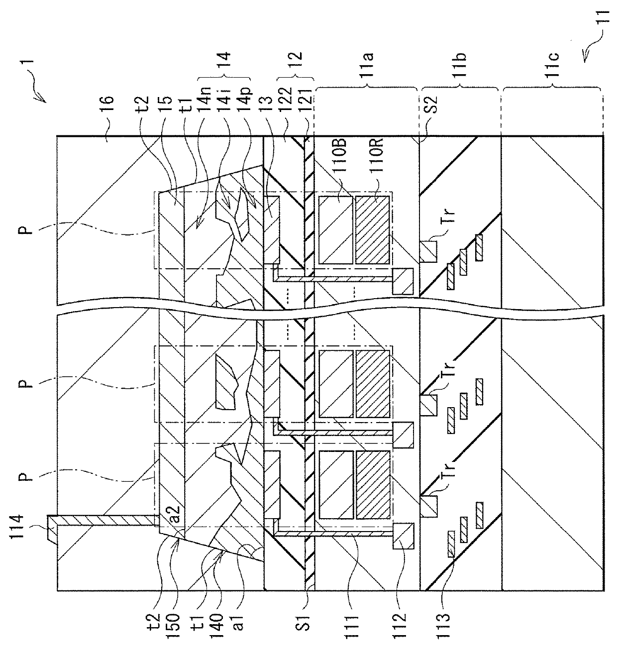
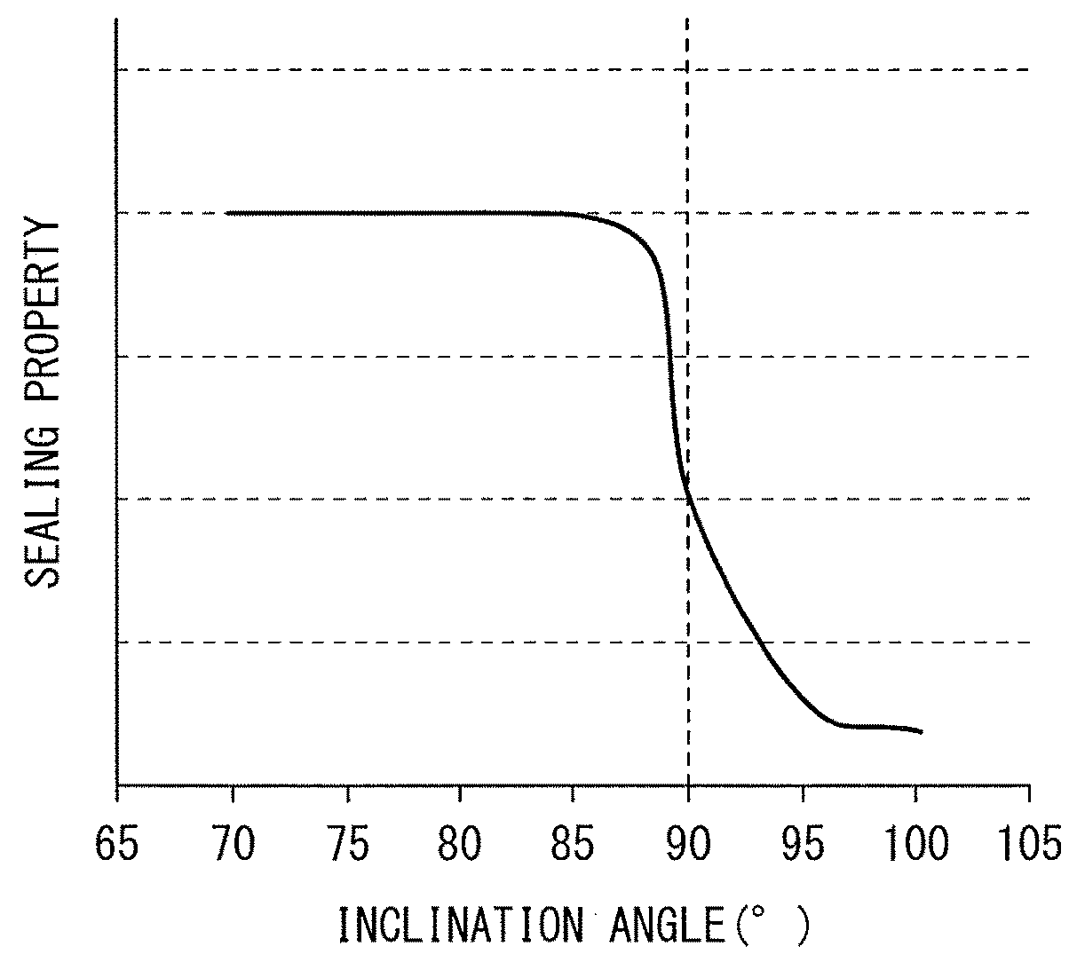
1. First embodiment (an example of a solid-state imaging device including an inclined surface on a side wall of an organic photoelectric conversion film)

2. Modification examples 1-1 and 1-2 (examples in which an inclination angle of the side wall of the organic photoelectric conversion film and an inclination angle of a side wall of a second electrode are different from each other)

modification example 2 (

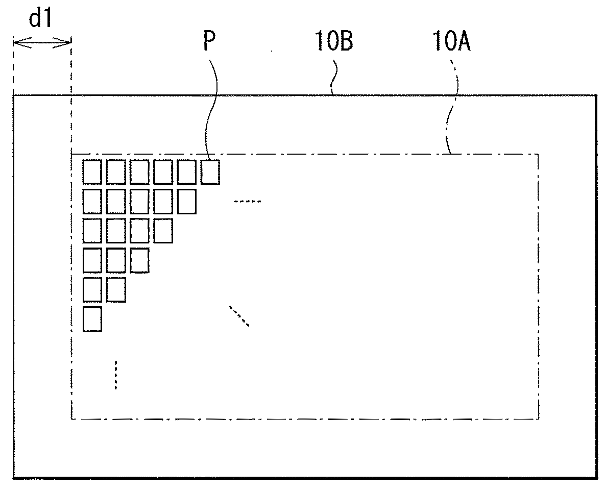
3. Modification example 2 (an example in which a plurality of organic photoelectric conversion films are formed separately for respective pixels)

second embodiment (

4. Second embodiment (an example of a solid-state imaging device including a second sealing film between a side wall of an organic photoelectric conversion film and a first sealing film)

5. Modification examples 3-1 to 3-3 (other configuration examples including the second sealing film)


PUM


Abstract

A solid-state imaging device includes: a plurality of pixels each including a first electrode, an organic photoelectric conversion film, and a second electrode in this order on a substrate, the organic photoelectric conversion film including a first inclined surface on a side wall; and a first sealing film formed, on the plurality of pixels, to cover the side wall of the organic photoelectric conversion film and the second electrode.

Description

TECHNICAL FIELD[0001]The present disclosure relates to a solid-state imaging device such as a CCD (Charge Coupled Device) image sensor and a CMOS (Complementary Metal Oxide Semiconductor) image sensor, and to a method of manufacturing the solid-state imaging device.BACKGROUND ART[0002]In recent years, in a solid-state imaging device such as a CCD image sensor and a CMOS image sensor, the number of photons entering a unit pixel is decreased with reduction of a pixel size, which deteriorates sensitivity and an S / N ratio as a result. Further, in such a solid-state imaging device, pixels of three primary colors are often two-dimensionally arranged typically with use of color filters of primary colors of red, green, blue, or other colors. In a case where the color filters are used, however, optical loss occurs to deteriorate sensitivity. For example, in a red pixel, green light and blue light are not photoelectrically converted because the green light and the blue light do not pass throu...

Claims


Application Information

Patent Timeline
IPC IPC(8): H01L27/30H01L51/44H01L51/42H01L27/28
CPCH01L27/307H01L51/448H01L51/442H01L51/4293H01L51/4273H01L27/286H01L27/281H01L51/0072Y02E10/549H01L27/14645H01L27/14667Y02P70/50H04N25/70H04N23/10H10K39/32H10K30/40H10K30/88H01L27/146H10K19/20H10K19/201H10K30/82H10K30/353H10K85/6572
Inventor JOEI, MASAHIRO
Owner SONY SEMICON SOLUTIONS CORP
Why Eureka
Try Eureka