Semiconductor chip and semiconductor module including the same
Active Publication Date: 2018-10-11
DENSO CORP
View PDF1 Cites 5 Cited by
Summary
Abstract
Description
Claims
Application Information
AI Technical Summary
This helps you quickly interpret patents by identifying the three key elements:
Problems solved by technology
Method used
Benefits of technology
Benefits of technology
The present patent aims to provide a semiconductor chip that can prevent malfunctions of a switching element. To achieve this, the chip has first and second control terminals that are connected to controls pads for controlling the current flow. This configuration helps to restrict an increase in potential at the control pad that could cause malfunctions in both the first and second chips. Overall, this patent helps to ensure the reliability and stability of the semiconductor chip.
Problems solved by technology
When the control current flows from the gate terminal to the Kelvin-emitter terminal, a voltage applied to the gate pad increases to a switching-ON side of the IGBT element, which may give rise to a malfunction.
Method used
Image
Click on the blue label to locate the original text in one second.
Reading with bidirectional positioning of images and text.
Examples
first embodiment
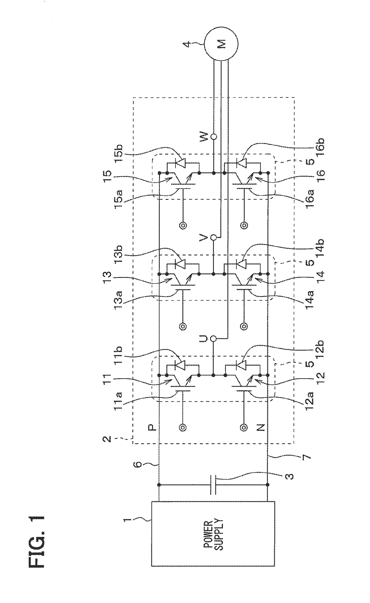
[0027]A first embodiment will be described. The present embodiment will describe an example where a technical idea of the present disclosure is applied to a semiconductor module forming a three-phase motor driving inverter.
[0028]A circuit configuration of the inverter will be described first. The inverter AC-drives a three-phase motor 4 as a load according to a DC power supply, and has a power-supply portion 1 including a step-up circuit, an inverter output circuit 2, and a capacitor 3 disposed in parallel between the power-supply portion 1 and the inverter output circuit 2. The capacitor 3 is a smoothingcapacitor and provided to form a constant power-supply voltage by reducing a noise influence of the power-supply portion (step-up circuit) 1. The inverter output circuit 2 includes serially-connected upper arms 11, 13, and 15 and lower arms 12, 14, and 16 of three phases which are connected in parallel phase by phase, and applies intermediate potential between the upper arms 11, 13...
second embodiment
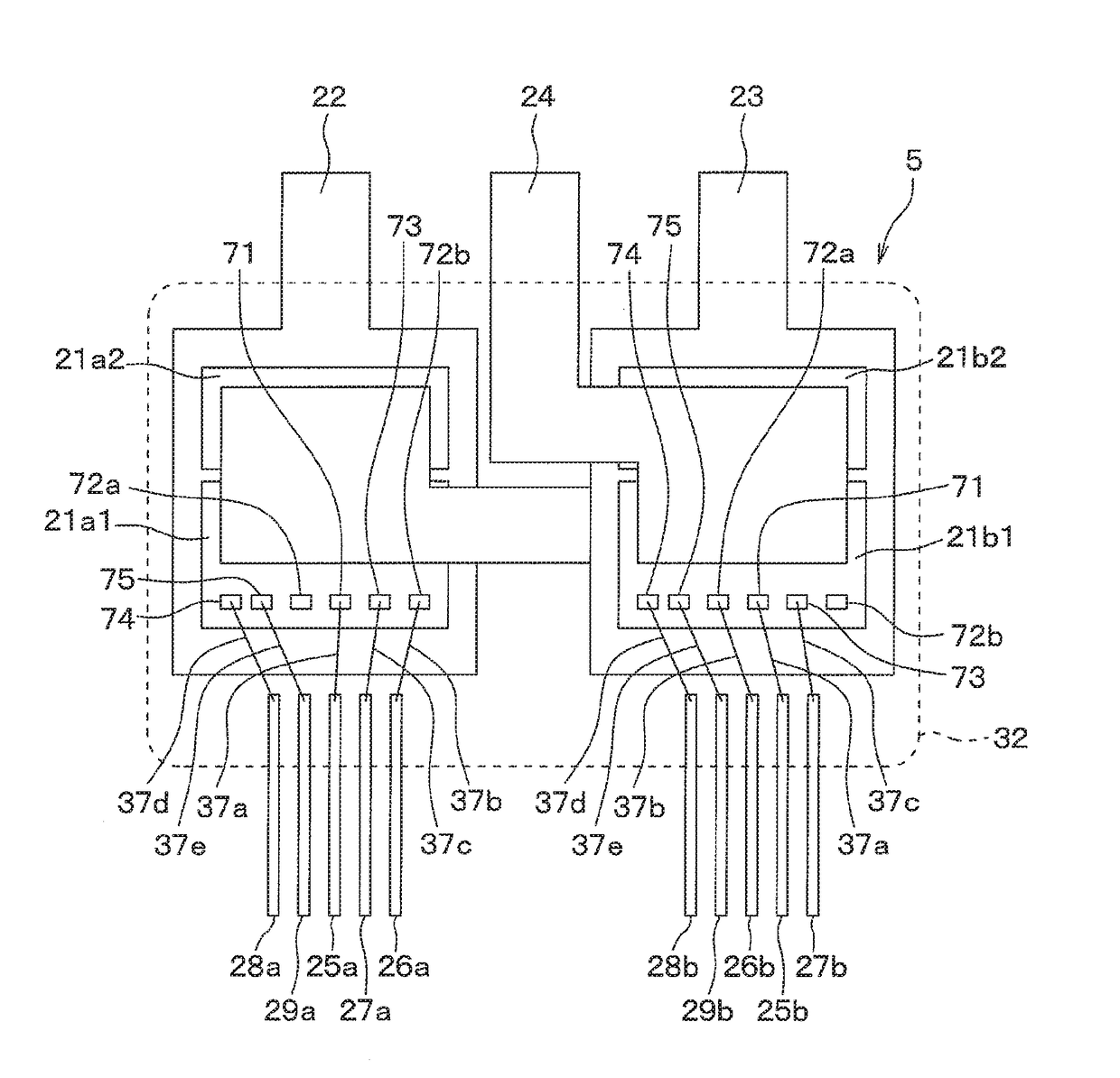
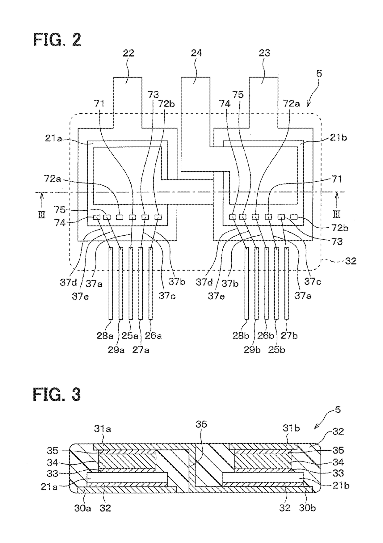
[0072]A second embodiment will now be described. The present embodiment is different from the first embodiment above in that each of semiconductor chips 21a and 21b is provided with a single Kelvin-emitter pad 72 and two gate pads 71 disposed to have the Kelvin-emitter pad 72 in between. A rest of the configuration is same as the configuration of the first embodiment above and a description is not repeated herein.
[0073]As is shown in FIG. 7, in the present embodiment, the semiconductor chip 21a is provided with the single Kelvin-emitter pad 72 alone. The semiconductor chip 21a is also provided with first and second gage pads 71a and 72b to have the Kelvin-emitter pad 72 in between. A configuration of the semiconductor chip 21b is same as the configuration of the semiconductor chip 21a.
[0074]Even when the semiconductor chips 21a and 21b are configured as above, by connecting gate terminals 25a and 25b, respectively, to one and the other one of the first and second gate pad 71a and 7...
third embodiment
[0075]A third embodiment will now be described. The present embodiment is different from the first embodiment above in that IGBT elements 11a and 12a and FWD elements 11b and 12b are provided to different chips. A rest of the configuration is same as the configuration of the first embodiment above and a description is not repeated herein.
[0076]As is shown in FIG. 8, in the present embodiment, the IGBT element 11a is provided to a semiconductor chip 21a1 whereas the FWD element 11b is provided to a semiconductor chip 21a2 on a side of an upper arm 11. In short, the IGBT element 11a and the FWD element 11b are provided to different semiconductor chips.
[0077]Likewise, the IGBT element 12a is provided to a semiconductor chip 21b1 whereas the FWD element 12b is provided to a semiconductor chip 21b2 on a side of a lower arm 12, As in the first embodiment above, each of the semiconductor chips 21a1 and 21b1 is provided with a gate pad 71, first and second Kelvin-emitter pads 72a and 72b, a...
PUM
Abstract
The present disclosure provides a semiconductorchip. The semiconductorchip includes a switching element having a gate electrode, a first pad, and a second pad. The first control pad is electrically connected to the gate electrode and applied with a voltage controlling the switching element to switch on or switch off. The second control pad provides a current path of a control current flowing between the first control pad and the second control pad when the switching element is in a switch-on state. One of the first control pad or the second control pad includes two pad components and a remaining one of the first control pad or the second control pad is disposed between the two pad components of the one of the first control pad or the second control pad.
Description
CROSS REFERENCE TO RELATED APPLICATION[0001]This application is based on Japanese Patent Application No. 2015-126785 filed on Jun. 24, 2015, the disclosure of which is incorporated herein by reference.TECHNICAL FIELD[0002]The present disclosure relates to a semiconductorchip having multiple pads to be connected to control terminals, and also relates to a semiconductor module including such a semiconductor chip.BACKGROUND ART[0003]A semiconductor module having so-called 2-in-1 structure is proposed in, for example, Patent Literature 1 as a semiconductor module forming an inverter. The proposed semiconductor module includes a semiconductor chip having a switching element forming an upper arm and another semiconductor chip having a switching element forming a lower arm. The switching elements of the respective semiconductor chips are connected in series. In the proposed semiconductor module, the respective semiconductor chips have a common configuration and each is provided with an IG...
Claims
Application Information
Patent Timeline
Application Date:The date an application was filed.
Publication Date:The date a patent or application was officially published.
First Publication Date:The earliest publication date of a patent with the same application number.
Issue Date:Publication date of the patent grant document.
PCT Entry Date:The Entry date of PCT National Phase.
Estimated Expiry Date:The statutory expiry date of a patent right according to the Patent Law, and it is the longest term of protection that the patent right can achieve without the termination of the patent right due to other reasons(Term extension factor has been taken into account ).
Invalid Date:Actual expiry date is based on effective date or publication date of legal transaction data of invalid patent.

