Systems and methods for the patterning of material substrates

a technology of material substrates and patterns, applied in the field of system and method for the patterning of material substrates, can solve the problems of not being compatible with many materials or integrated systems, using high-temperature annealing, and and achieving the effect of preventing the single-step fabrication of multi-functional systems and appreciable thermal stresses and temperature gradients

Active Publication Date: 2018-12-13
THE AEROSPACE CORPORATION
View PDF32 Cites 3 Cited by
  • Summary
  • Abstract
  • Description
  • Claims
  • Application Information

AI Technical Summary

Benefits of technology

[0004]However, continued exposure of at least a portion of the sample or component to such high temperatures can result in appreciable thermal stresses and temperature gradients in the sample. As a result, the use of high-temperature annealing may not be compatible with many materials or integrated systems, such as electronics, optics, plastics, organic substrates and thin films. In addition, the need to utilize high temperature annealing in conjunction with optical patterning precludes the single-step fabrication of multi-functional systems. Thus, current processing and manufacturing technologies rely on the separate fabrication of discrete elements, each with their own function, followed by post-process alignment and assembly.
[0005]The embodiments described herein enable a single step approach to create and / or modify material substrates, such as GCs, by patterning, or “writing” structures and phases into the substrates in-situ. Using this approach, the material substrate may have a wide range of phases and compositions having various functionalities, structures, and properties. For example, in one embodiment, a material modification assembly is provided. The material modification assembly includes a computing device that is configured to generate at least one process script for the modification to the material substrate and to generate at least one pattern script that corresponds to the process script, for the modification to the material substrate. The computing device is also configured to merge the generated process script with the corresponding generated pattern script and to generate a plurality of command signals that are based on the merged generated process script and the corresponding generated pattern script. An energy source is configured to couple to the computing device, wherein the energy source is further configured to generate a plurality of light beams based on at least one of the generated command signals. A motion control drive is configured to couple to the computing device and the energy source, wherein the motion control drive is further configured to generate a waveform type indicator based on the at least one of the plurality of command signals. A waveform apparatus is configured to couple to the computing device, the energy source, and the motion control drive. The waveform apparatus is further configured to generate at least one waveform signal based on the at least one of the generated plurality of command signals and the waveform type indicator.
[0006]At least one modulating component is configured to couple to the computing device, the waveform apparatus, and the energy source, wherein the modulating component is further configured to modulate the generated plurality of light beams with the waveform signal based on at least one of the generated command signals. In addition, an optical assembly is configured to couple to the modulating component, and the optical assembly is further configured to apply the modulated plurality of light beams to the material substrate. At least one motion stage encoder is configured to couple to the motion control drive and the optical assembly, wherein the motion stage encoder is further configured to provide at least one three dimensional (3D) coordinate position of the optical assembly with respect to the motion control drive in order to coordinate application of the modulated light beams with a predefined spatial location.
[0007]In another embodiment, a method to modify at least one material substrate is provided. At least one process script is generated, via a computing device, to modify the material substrate. At least one pattern script that corresponds to the process script is generated, via the computing device, to modify the material substrate. The process script is merged with the corresponding pattern script. A plurality of command signals are generated, wherein the command signals are based on the merged process script and the corresponding pattern script. A plurality of light beams are generated, via an energy source, based on at least one of the command signals. A waveform type indicator is generated, via a motion control drive, based on at least one of the command signals. At least one waveform signal is generated, via a waveform apparatus, based on at least one of the command signals. The light beams are then modulated with the waveform signal, via a modulating component. The modulating is based on at least one of the command signals. The modulated light beams are applied to a GC substrate, via an optical assembly. At least one three dimensional (3D) coordinate position of the optical assembly with respect to the motion control drive is provided, via a motion stage encoder, in order to coordinate application of the modulated light beams with a predefined spatial location.

Problems solved by technology

However, continued exposure of at least a portion of the sample or component to such high temperatures can result in appreciable thermal stresses and temperature gradients in the sample.
As a result, the use of high-temperature annealing may not be compatible with many materials or integrated systems, such as electronics, optics, plastics, organic substrates and thin films.
In addition, the need to utilize high temperature annealing in conjunction with optical patterning precludes the single-step fabrication of multi-functional systems.

Method used


Image

  • Systems and methods for the patterning of material substrates
  • Systems and methods for the patterning of material substrates
  • Systems and methods for the patterning of material substrates

Examples


Embodiment Construction

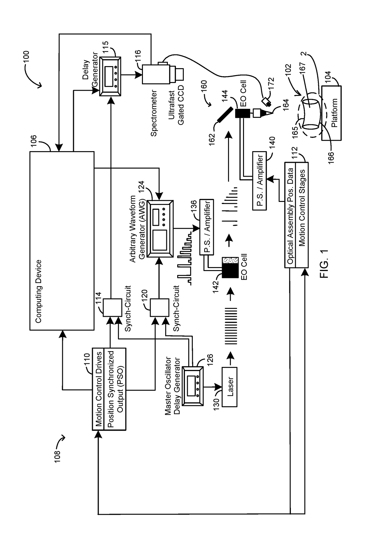
[0014]The embodiments described herein enable the in-situ patterning of material substrates, such as GC substrates, with various phases, such that the GC substrate can be imbued with various functionalities and can create complex highly integrated systems within the GC substrate. Such systems can include photonic, bionic, and electronic systems among others. The embodiments described herein include, for example, the use of laser scripted pulse modulation techniques to directly transform the amorphous phases of the GC matrix into discrete etchable (soluble) phases, thus inducing site-selective phase conversion during the laser patterning process. Such techniques enable for the control and definition of variations in the electrical and optical character, mechanical compliance, and chemical solubility of the GC substrate. The laser genotype modulation approach can be translated to other photo-structurable GCs and a wide array of other related materials, including organic-inorganic hybr...


PUM

PropertyMeasurementUnit
energyaaaaaaaaaa
distanceaaaaaaaaaa
porosityaaaaaaaaaa

Abstract

A system includes a computing device that generates at least one process script for the modification to a glass ceramic substrate and at least one pattern script that corresponds to the process script. The computing device also merges the process script with the pattern script and generates a plurality of command signals that are based on the merged process and pattern scripts. An energy source generates a plurality of light beams based on the generated command signal(s). A waveform apparatus generates at least one waveform signal to customize the generated light beams based on the generated command signal(s). At least one modulating component modulates the generated light beams based on generated command signal(s). An optical assembly is configured to apply the modulated plurality of light beams to the glass ceramic substrate. At least one motion stage encoder is configured to provide at least one three dimensional (3D) coordinate position of the optical assembly with respect to the motion control drive in order to coordinate application of the modulated light beams with a predefined spatial location.

Description

RELATED AND CO-PENDING APPLICATION[0001]This application is a continuation-in-part of and claims priority to co-pending U.S. patent application Ser. No. 15 / 469,132 entitled SYSTEMS AND METHODS FOR MODIFYING MATERIAL SUBSTRATES (attorney docket no. D-802 (F9959-00021)) filed Mar. 24, 2017, which is a continuation in part of and claims priority to U.S. patent application Ser. No. 14 / 163,712 entitled MATERIAL MODIFICATION ASSEMBLY AND METHOD FOR USE IN THE MODIFICATION OF MATERIAL SUBSTRATES (attorney docket no. D-758 (F9959-00012)) filed Jan. 24, 2014, which is a continuation-in-part of and claims priority to U.S. patent application Ser. No. 13 / 767,055 entitled BONE GROWTH ENHANCING IMPLANT (attorney docket no. DN0209) filed Feb. 14, 2013 and issued as U.S. Pat. No. 8,679,189 on Mar. 25, 2014, which claims the benefit of U.S. Provisional Application 61 / 763,223, filed Feb. 11, 2013, the disclosures of which are incorporated herein by reference in their entirety.BACKGROUND[0002]At least...

Claims


Application Information

Patent Timeline
Patent Type & Authority Applications(United States)
IPC IPC(8): G05B19/4155
CPCG05B19/4155G05B2219/45041C03C23/0025
Inventor LIVINGSTON, FRANK EDWARD
Owner THE AEROSPACE CORPORATION
Why Eureka
Try Eureka