Reticle fabrication method

a technology of reticles and fabrication methods, applied in the field of reticle fabrication methods, can solve the problems of large amount of data that is handled at the time of writing circuit patterns on reticles, significant increases in the time and cost needed to fabricate reticles, and reduce the number of reticles. to be manufactured, so as to prevent the fabrication of defective reticles, shorten the reticle fabrication period, and simplify the reticle inspection process

Inactive Publication Date: 2005-08-02
NEC CORP
View PDF12 Cites 3 Cited by
  • Summary
  • Abstract
  • Description
  • Claims
  • Application Information

AI Technical Summary

Benefits of technology

[0011]Accordingly, it is an object of the invention to provide a reticle fabrication method which simplifies a reticle inspection process, improves the effective availability factors of devices needed for reticle fabrication, such as an EB write device and a reticle inspection device, shortens the time needed for reticle fabrication and cuts down the fabrication cost by detecting a defect, such as a data conversion error included in EB write data like a circuit pattern to be written on a reticle
[0018]The reticle fabrication methods according to the invention use two data conversion devices to separately generate EB write data for writing a pattern on a reticle and inspection data for inspecting the reticle from CAD data or EB write data through data conversion and allow the data verification device to verify if there is a data conversion error contained in those data before EB writing to fabricate the reticle. This can reliably prevent fabrication of a defective reticle originated from a data conversion error. In case where a data conversion error is detected by the data verification device, the cause for the data conversion error occurred in each data conversion device can be found out instantaneously before reticle writing, it is possible to avoid writing a wasteful defective reticle, simplify the reticle inspection process and shorten the reticle fabrication period. This can lead to a noticeable reduction in reticle fabrication cost. Even in case where the reticle inspection device detects a defect on an EB-written and developed reticle, it is apparent that the cause for the defect is not a data conversion error, thus making it extremely easy to find out the cause for the defect. Therefore, not only the cause for a defect, such as a data conversion error, which occurs at an early stage of the fabrication process, but also the cause for a defect which is generated at a later stage of the fabrication process, such as the EB writing process or the developing process, can be found out easily at an early stage after the end of the process where such a defect has occurred.

Problems solved by technology

In this respect, circuit patterns to be written on reticles become extremely complex as well as become microfabricated more finely.
The amount of data that is handled at the time of writing a circuit pattern on a reticle becomes very huge due to the microfabrication and complexity of circuit patterns to be written on reticles.
This leads to significant increases in the time and cost needed to fabricate reticles.
It is therefore expected that increases in the time and cost needed to fabricate reticles become more prominent.
While the prior art can detect a defect at the time of writing a circuit pattern on a reticle, however, it cannot specify the cause for a defect, if detected.
Further, the fabrication cost would be increased significantly if the EB writing device which, like the reticle inspection device, is expensive and should face with an issue of the effective availability factor is operated to write a circuit pattern on a reticle based on EB write data containing a data conversion error.
Furthermore, the reticle that is fabricated based on such erroneous EB write data would be wasted.
This prior art does not however achieve the demanded early detection of a data conversion error in a data conversion device.
Therefore, the last prior art document also fails to disclose any specific means of solving the problem of the elongation of the reticle fabrication process and the cost increase both originated from such a data conversion error.

Method used


Image

  • Reticle fabrication method
  • Reticle fabrication method
  • Reticle fabrication method

Examples


first embodiment

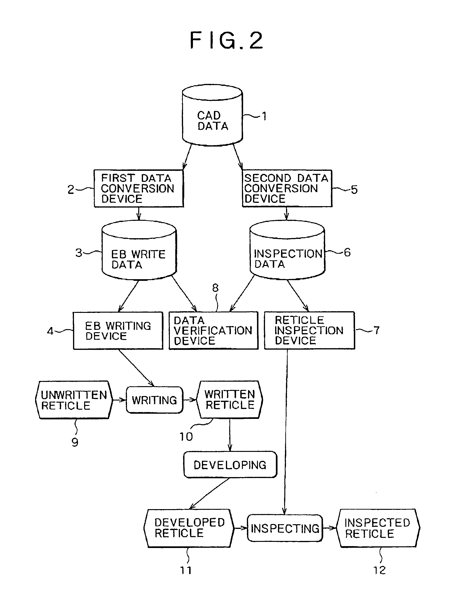
[0030]FIG. 2 is a flowchart illustrating a reticle fabrication method according to the invention. In the embodiment, CAD data 1 or reticle design data is input to a first data conversion device 2 and a second data conversion device 5. The first data conversion device 2 performs a conversion process, such as rotation, magnification, reduction, expansion or contraction, on a figure pattern contained in the CAD data 1 and performs format conversion on the resultant data to thereby convert the CAD data 1 to EB write data 3. The second data conversion device 5 performs a conversion process and format conversion on the figure pattern contained in the CAD data 1, which are similar to those done by the first data conversion device 2, thereby converting the CAD data 1 to inspection data 6. The EB write data 3 and the inspection data 6 are input to a data verification device 8. The data verification device 8 verifies if the first data conversion device 2 and the second data conversion device ...

fourth embodiment

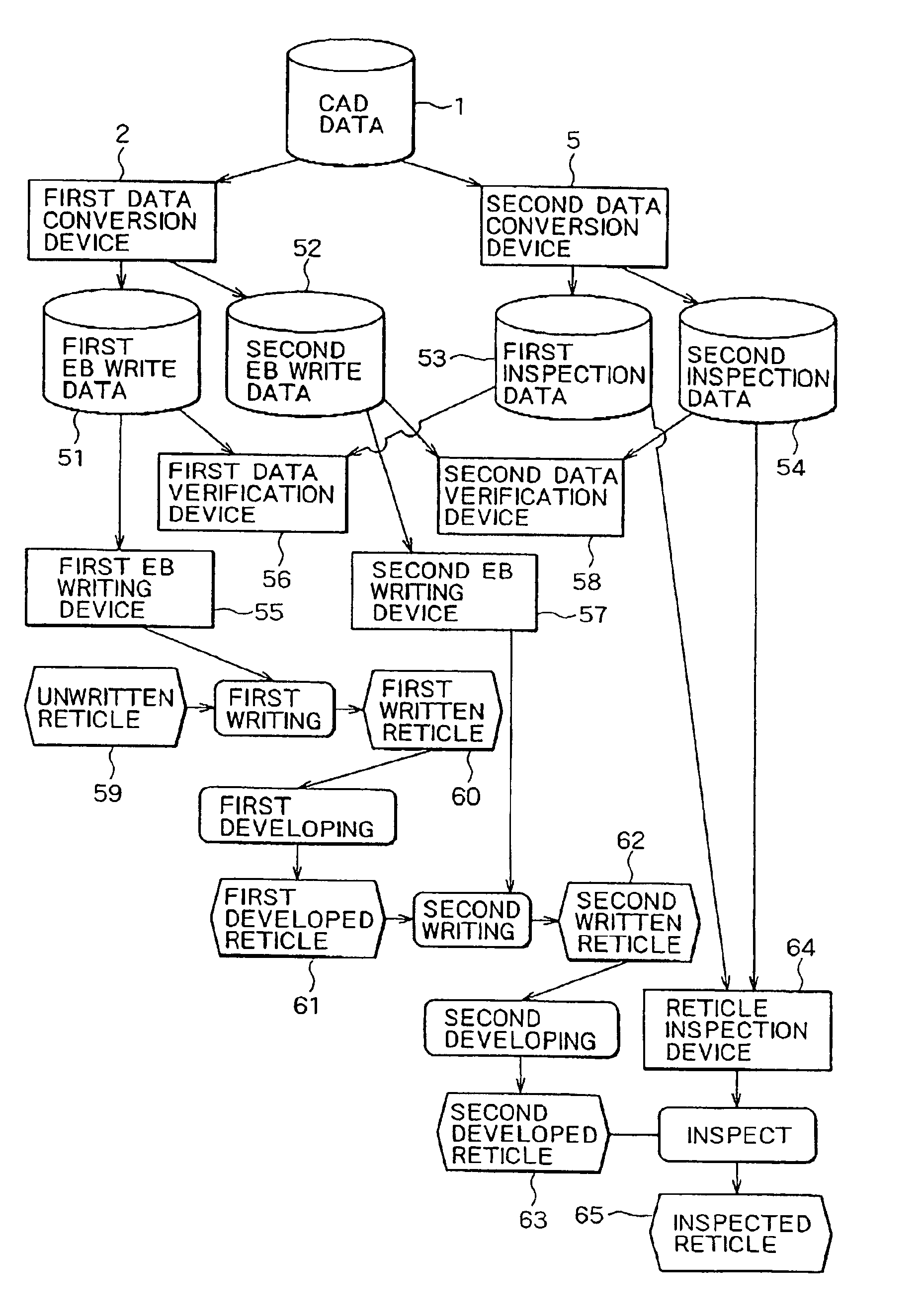
[0040]A reticle fabrication method according to the invention will be discussed below referring to the flowchart illustrated in FIG. 10. This embodiment is suitable for use in a reticle fabrication method which performs each of the EB writing process and developing process on a single reticle twice as done for a tritone mask and a phase shift mask which are used in super resolution techniques, such as OPC and phase shifting. In the embodiment, CAD data 1 or reticle design data is input to the first data conversion device 2 and the second data conversion device 5. The first data conversion device 2 performs a conversion process, such as rotation, magnification, reduction, expansion or contraction, on a figure pattern contained in the CAD data 1 and performs format conversion on the resultant data to thereby convert the CAD data 1 to first EB write data 51 and second EB write data 52. The second data conversion device 5 performs a conversion process and format conversion on the figure...


PUM

PropertyMeasurementUnit
electron beam writeaaaaaaaaaa
light transmittiveaaaaaaaaaa
speedaaaaaaaaaa

Abstract

CAD (Computer Aided Design) data which is reticle design data is input to first and second data conversion devices which respectively convert the CAD data to electron beam (EB) write data and inspection data. The EB write data and inspection data output are input to a data verification device to verify whether or not there is a data conversion error. If no data conversion error is detected by the data verification device, an EB writing device writes a pattern on an unwritten reticle with an electron beam based on the EB write data and develops the reticle, after which the fabricated developed reticle is inspected by a reticle inspection device. As a defect, such as a data conversion error contained in EB write data is detected before fabrication of a reticle, the reticle inspection process is simplified, the effective availability factors of the EB writing device and reticle inspection device and the time needed to fabricate a reticle is made shorter, thereby reducing the fabrication cost.

Description

FIELD OF THE INVENTION[0001]The present invention relates to a method of fabricating masks for a photolithography process performed on a reticle or the like which is used in fabricating a semiconductor integrated circuit device.DESCRIPTION OF RELATED ART[0002]In the photolithography process that is essential in the fabrication process for a semiconductor integrated circuit device, generally, a mask called a reticle which is acquired by writing the design pattern of a desired semiconductor integrated circuit on a light transmittive substrate, such as a quartz glass substrate, with a light shielding material such as chromium (Cr) is used as a master plate. The present photolithography technology generally employs a scheme of transferring a circuit pattern written on the reticle onto a semiconductor wafer with a photoresist applied thereto by reduction exposure by a factor of 4 to a factor of 5.[0003]The microfabrication technology for semiconductor integrated circuits demands microfab...

Claims


Application Information

Patent Timeline
Patent Type & Authority Patents(United States)
IPC IPC(8): G03F1/08G06F17/50H01L21/027H01L21/02G03F1/68G03F1/84G03F7/20H01J37/302
CPCG03F1/78G03F1/84G03F7/2063H01J37/3023H01J2237/30455H01J2237/3175G03F1/68
Inventor YOSHIMURA, TAKASHIBASHOMATSU, TAKESHI
Owner NEC CORP
Why Eureka
Try Eureka