Wafer Lithographic Mask and Wafer Lithography Method Using The Same

a lithographic mask and shielding mask technology, applied in the field of wafer lithographic shielding mask and wafer lithography method using the same, can solve the problems of destroying many other dice in the same wafer, affecting the production efficiency of the reticle (mask) tooling, and affecting the production efficiency of the reticle. the effect of saving the production cost and avoiding the fabrication of undesired chips on the wafer

Active Publication Date: 2007-09-20
YUAN ZE UNIV
View PDF8 Cites 3 Cited by
  • Summary
  • Abstract
  • Description
  • Claims
  • Application Information

AI Technical Summary

Benefits of technology

[0009]The wafer photolithography method provided by the present invention can, to a certain extent, avoid fabricating undesired chips on the wafer using the MPW reticle. When some projects later find out that their chips fabricated with MPW work pretty well and decide to go with volume production, they can reuse the MPW reticle to save reticle (mask) tooling cost and use the shielding mask disclosed in the present invention to save wafer production cost.

Problems solved by technology

However, as chips of various lengths or widths are placed in one reticle, in order to reduce the tooling cost of the reticle and the production cost of wafers, the problems of floorplanning and dicing of MPW arise.
Though the tooling cost of the reticle 101 of the MPW can be shared by individual projects, comparing the MPW reticle with the conventional reticle which consists of one or several copies of the layout patterns of a single chip, the cost of the lithographic process for the MPW and the cost of fabricating the required wafers are greatly increased.
Due to this limitation, sawing a certain die out of a wafer may frequently destroy many other dice in the same wafer.
As the tooling cost of reticle increases dramatically with advanced semiconductor process technology, the potentiality of using MPW reticle for larger volume production also increases considerably.
However, because different production volume requirements exist among the projects participating in an MPW fabrication run, in order to produce enough bare dice for the projects with considerably large production volumes, excessive number of wafers will be fabricated.
These wafers produce unwanted dice for the projects with smaller production volumes.
In view of the above, the tremendous increase in the fabricating cost of the MPW is caused by the fabrication of some unwanted dice or dice destroyed by wafer sawing.
This is expensive and inefficient because this approach will also fabricate the dice not belonging to the underlying project.
This is also very expensive if the production volume is not large enough to justify such an investment.

Method used


Image

  • Wafer Lithographic Mask and Wafer Lithography Method Using The Same
  • Wafer Lithographic Mask and Wafer Lithography Method Using The Same
  • Wafer Lithographic Mask and Wafer Lithography Method Using The Same

Examples


Embodiment Construction

[0013]The appended drawings will be used to clearly disclose the technical characteristics of the present invention.

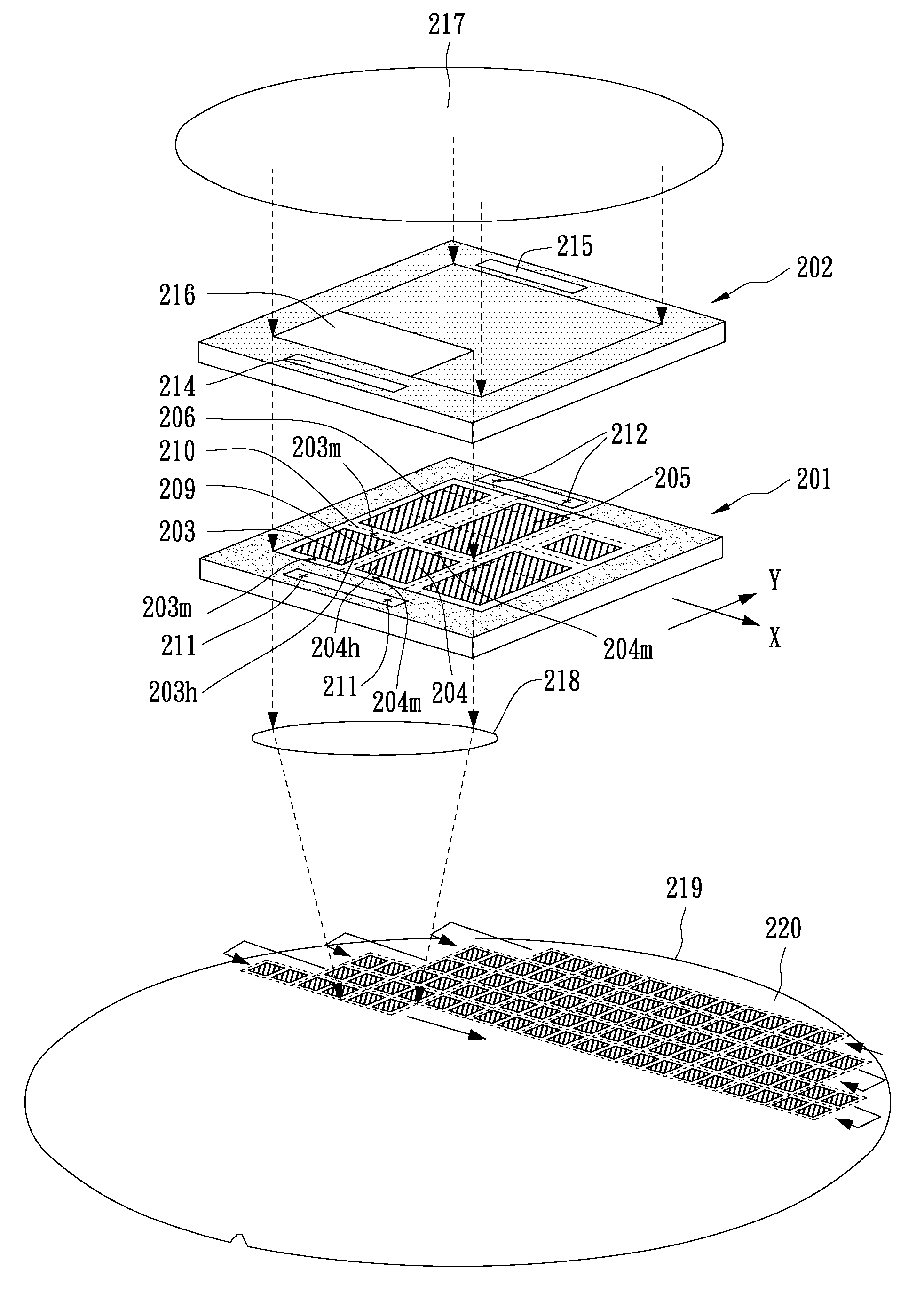
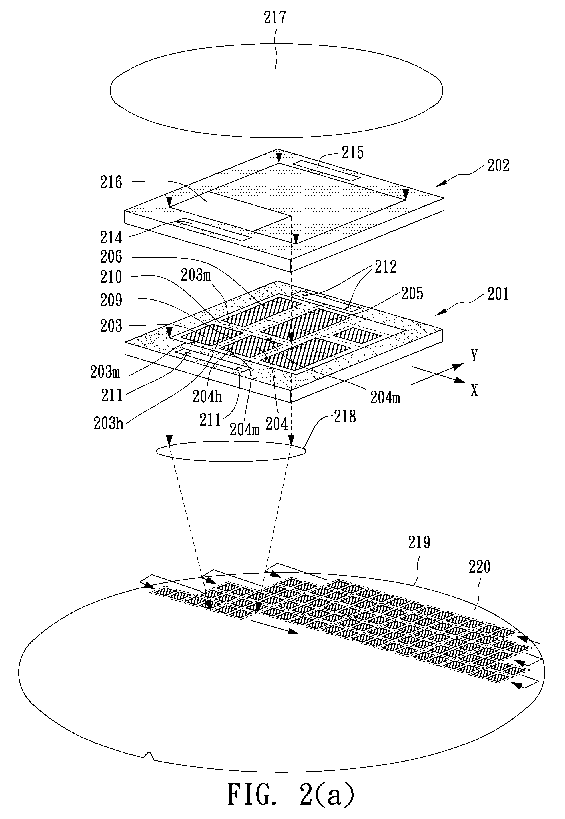
[0014]FIG. 2(a) is a lithographic apparatus according to an embodiment of the present invention. When an MPW reticle 201 is being fabricated, it is additionally provided with fine alignment marks for some projects on the reserved regions where a diamond blade will be applied, for example, fine alignment marks 203m and 204m on the reserved regions used for wafer sawing. The fine alignment marks are used to align the patterns to be exposed with the patterns already formed on the wafer, so as to achieve the fine alignment of the layout patterns to be fabricated.

[0015]First, the layout patterns of the chips to be fabricated are selected with reference to the floorplan of the MPW reticle 201. In the present embodiment, the chips 203 and 204 are selected to get exposure. The neighboring sides 203h and 204h of chips 203 and 204 have the same length and their bottom Y coordina...


PUM


Abstract

A wafer lithographic shielding mask for fabricating a multi-project wafer (MPW) and a wafer fabrication method using the same are disclosed. The mask including a light shielding layer and at least one transparent region is used to select the layout patterns of designated chips on an MPW reticle to be exposed onto the photoresist layer on the surface of the wafer. The lithography method of fabricating MPW mainly involves disposing a wafer lithographic shielding mask for selecting the exposure regions on the MPW reticle on the light transmission path from a lithographic light source to a wafer, e.g., between the MPW reticle and the lithographic light source or between the MPW reticle and the wafer, so as to prevent some undesired chips from being fabricated on the wafer using the MPW reticle, thereby decreasing the wafer production cost.

Description

BACKGROUND OF THE INVENTION[0001](A) Field of the Invention p The present invention relates to a wafer lithographic shielding mask and a wafer lithography method using the same, and more particularly to a lithographic shielding mask for multi-project wafers (MPW) and a wafer lithography method using the same.[0002](B) Description of the Related Art[0003]According to current techniques for fabricating MPW, layout patterns of several integrated circuits or chips from different projects are disposed in one reticle, so that the tooling cost of the reticle is shared by individual projects. The layout patterns for each chip refer to those required to be formed on the reticle for producing a working chip. However, as chips of various lengths or widths are placed in one reticle, in order to reduce the tooling cost of the reticle and the production cost of wafers, the problems of floorplanning and dicing of MPW arise. As to the floorplanning, the positions of the chips on the reticle must be...

Claims


Application Information

Patent Timeline
Patent Type & Authority Applications(United States)
IPC IPC(8): G03B27/58
CPCG03F7/70425G03B27/58
Inventor TSAI, SHIH CHENGLIN, RUNG BIN
Owner YUAN ZE UNIV
Why Eureka
Try Eureka