Supercharge Your Innovation With Domain-Expert AI Agents!

Gallium nitride semiconductor structure and process for fabricating thereof

a technology of gallium nitride and semiconductor structure, applied in the field of semiconductor structure, can solve the problems of insufficient thermal conductivity of sic substrate, inability to overcome heat load, and material cannot be widely used for electronic applications

Active Publication Date: 2018-12-20
ELTA SYST LTD
View PDF4 Cites 5 Cited by
  • Summary
  • Abstract
  • Description
  • Claims
  • Application Information

AI Technical Summary

Benefits of technology

The patent text discusses the need for a new way to remove heat from electronic and optics elements made using GaN semiconductors. The text concludes that this new structure would help improve the efficiency of heat removal.

Problems solved by technology

However, although this approach has been shown to be a viable solution for fabrication of GaN microwave devices, it still cannot overcome heat loads, and suffers from rather insufficient thermal conductivity of the SiC substrate.
Although natural diamond is an excellent thermal conductor, this material cannot be widely used for electronic applications due to its scarcity and cost.
However, integration of a CVD diamond introduces many challenges due to interface issues associated with material lattice mismatch and with different thermal expansion of the GaN and diamond layers, that can be a reason for bowing and warping of the GaN-on-diamond structure and its delamination.
Moreover, diamond-based composite substrates require careful attention to thermal resistance of the interface layer formed between the GaN and the diamond, which can diminish the benefits of using this high conductivity material.

Method used


Image

  • Gallium nitride semiconductor structure and process for fabricating thereof
  • Gallium nitride semiconductor structure and process for fabricating thereof
  • Gallium nitride semiconductor structure and process for fabricating thereof

Examples


Embodiment Construction

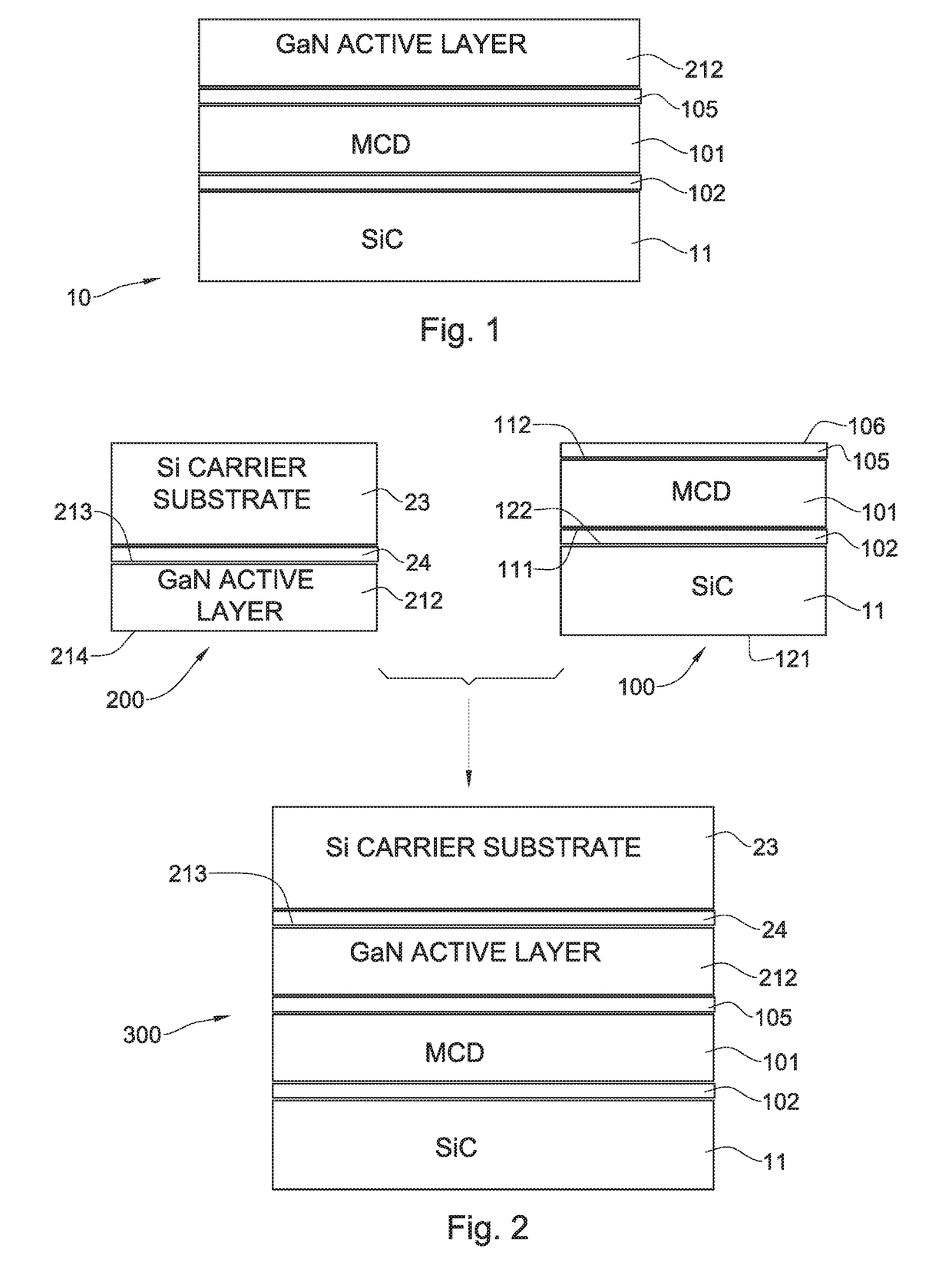
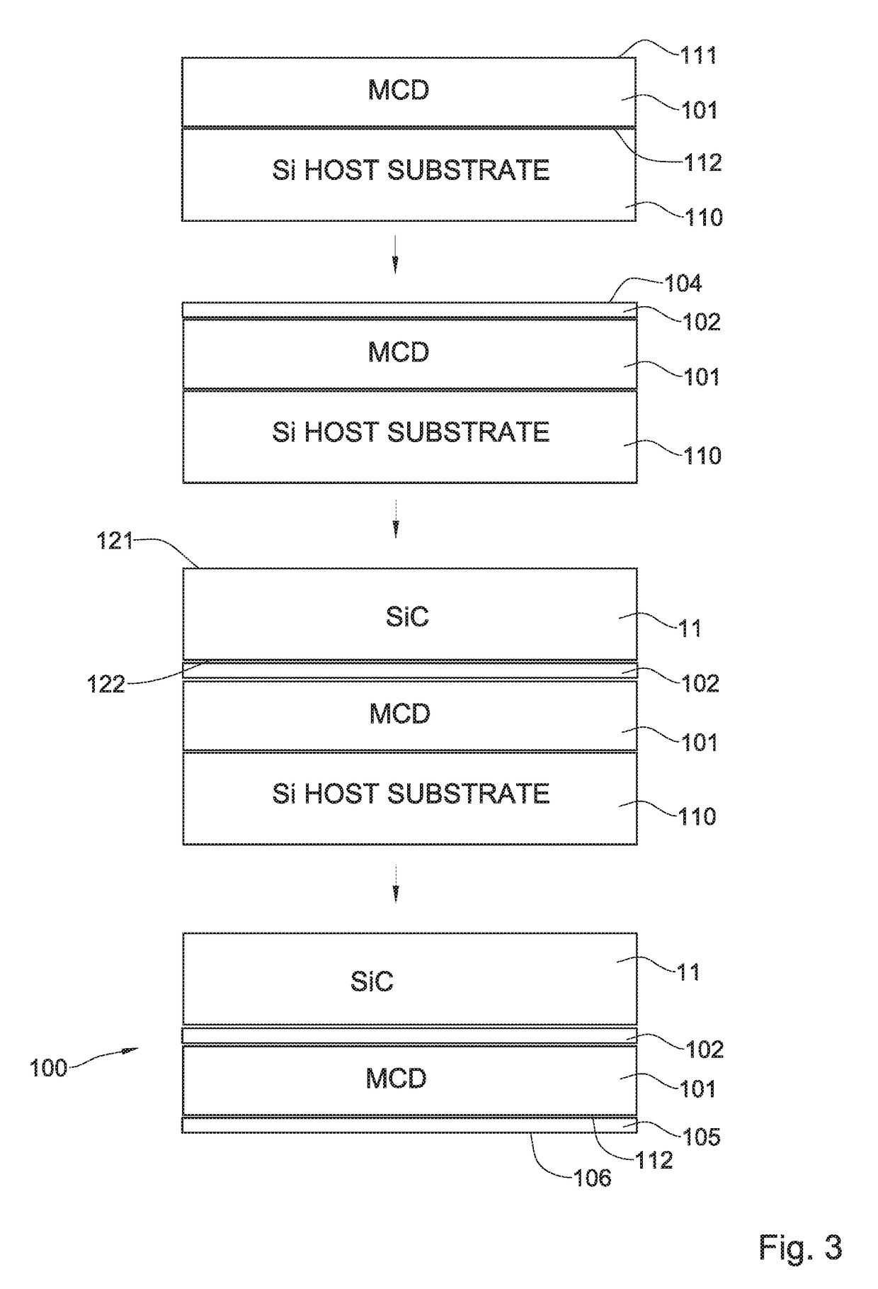
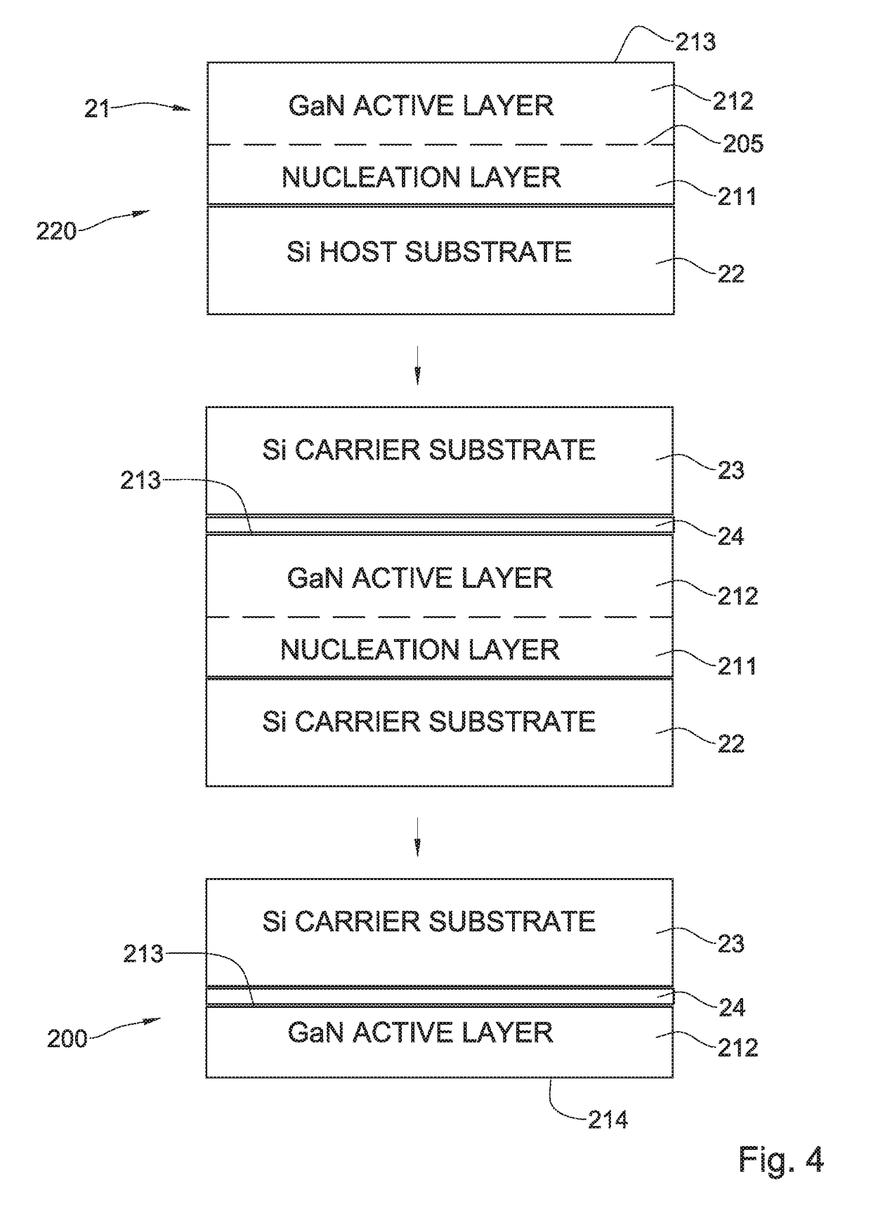
[0042]The principles of the semiconductor structure and fabrication method according to the present invention may be better understood with reference to the drawings and the accompanying description, wherein like reference numerals have been used throughout to designate identical elements. It is to be understood that these drawings, which are not necessarily to scale, are given for illustrative purposes only and are not intended to limit the scope of the invention. For example, the dimensions of some of the elements in the figures may be exaggerated relative to other elements to help improve understanding of various embodiments. In addition, the description and drawings do not necessarily require the order illustrated. It will be further appreciated that certain actions and / or steps may be described or depicted in a particular order of occurrence while those skilled in the art will understand that such specificity with respect to sequence is not actually required.

[0043]Embodiments o...


PUM


Abstract

A semiconductor substrate structure and process for fabrication of the semiconductor substrate structure are described. The semiconductor substrate structure includes a silicon carbide (SiC) wafer substrate, an active gallium nitride (GaN) layer and a layer of microcrystalline diamond (MCD) layer disposed between the SiC wafer substrate and the GaN active layer. The MCD) layer is bonded to the SiC wafer substrate and to the GaN active layer.

Description

FIELD OF THE INVENTION[0001]This invention relates to semiconductor structures and, more particularly to gallium nitride (GaN) semiconductor structures and processes for fabricating thereof.BACKGROUND OF THE INVENTION[0002]Gallium Nitride (GaN) is a wide-gap semiconductor that is used today for optoelectronic and electronic devices, such as visible light-emitting diodes and lasers, and high-power microwave electronic transistors. Such devices produce a high amount of heat requiring a heat spreader to be attached to GaN layers to ensure that electrical properties of the semiconductor remain within a safe temperature operating region. One of the known approaches is to use a GaN layer disposed on a SiC substrate configured for thermal management.[0003]For example, U.S. Pat. No. 9,111,750 to Kashyap et al. describes a monolithically integrated semiconductor assembly. The semiconductor assembly includes a substrate including silicon carbide (SiC), and a gallium nitride (GaN) semiconducto...

Claims


Application Information

Patent Timeline
IPC IPC(8): H01L29/66H01L29/20H01L29/16H01L21/02H01L21/20
CPCH01L29/66446H01L29/2003H01L29/1608H01L21/02378H01L21/0254H01L21/02527H01L21/0228H01L21/2007H01L33/0075H01L33/0093H01L21/02002H01L21/31051H01L21/185H01L21/0262H01L2924/1033
Inventor KAPLUN, JOSEPHHOULI ARBIV, BILHA
Owner ELTA SYST LTD
Features
  • R&D
  • Intellectual Property
  • Life Sciences
  • Materials
  • Tech Scout
  • Unparalleled Data Quality
  • Higher Quality Content
  • 60% Fewer Hallucinations
Learn More