
Magnetic memory

Active Publication Date: 2018-12-27
TDK CORPARATION
View PDF4 Cites 11 Cited by
  • Summary
  • Abstract
  • Description
  • Claims
  • Application Information

AI Technical Summary

Benefits of technology

The patent describes a way to integrate magnetoresistance elements using a pure spin current generated by spin-orbit interactions. This results in more efficient and effective integration of these elements.

Problems solved by technology

In the method of performing writing using a magnetic field, there is a limit to a current that can flow into a thin wiring and there is a risk of writing not being possible when an element size becomes smaller.

Method used


Image

  • Magnetic memory
  • Magnetic memory
  • Magnetic memory

Examples


first embodiment

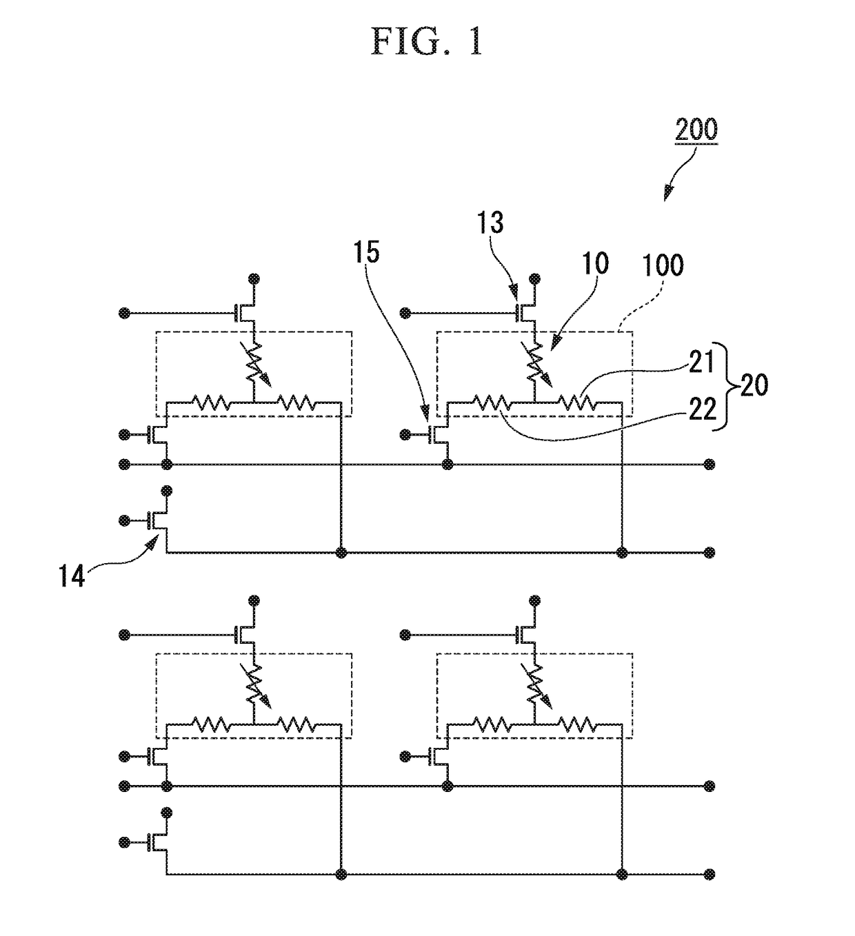
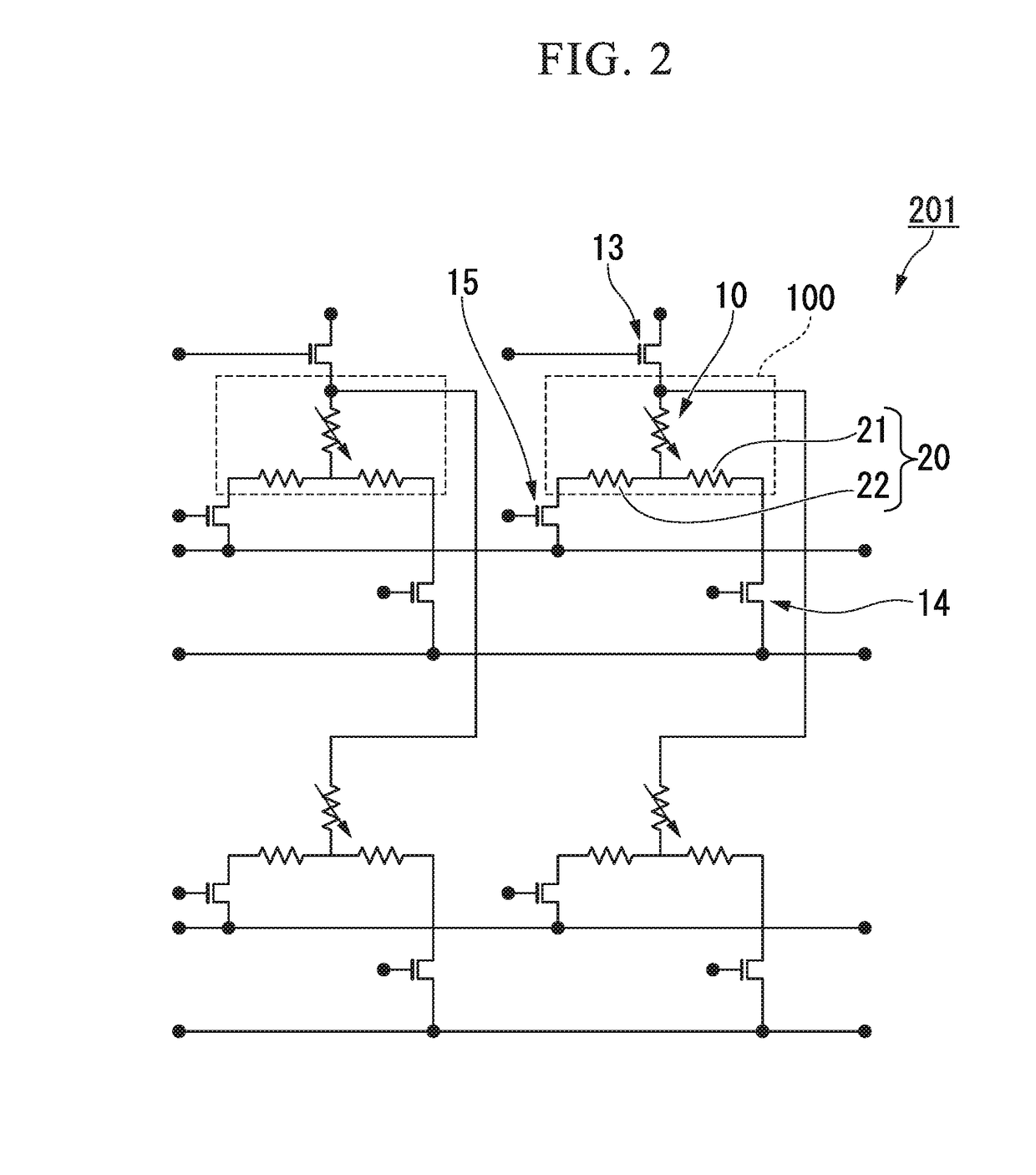
[0039]FIG. 1 and FIG. 2 are circuit diagrams of a magnetic memory according to the present embodiment. A magnetic memory 200 includes a plurality of drive elements 100. The drive element 100 includes a magnetoresistance effect element 10 and a spin-orbit torque wiring 20. In the circuits in FIG. 1 and FIG. 2, the spin-orbit torque wiring 20 is shown as resistors 21 and 22. Current leakage during writing and reading is low in both the magnetic memory 200 shown in FIG. 1 and a magnetic memory 201 shown in FIG. 2, which function as magnetic memories.

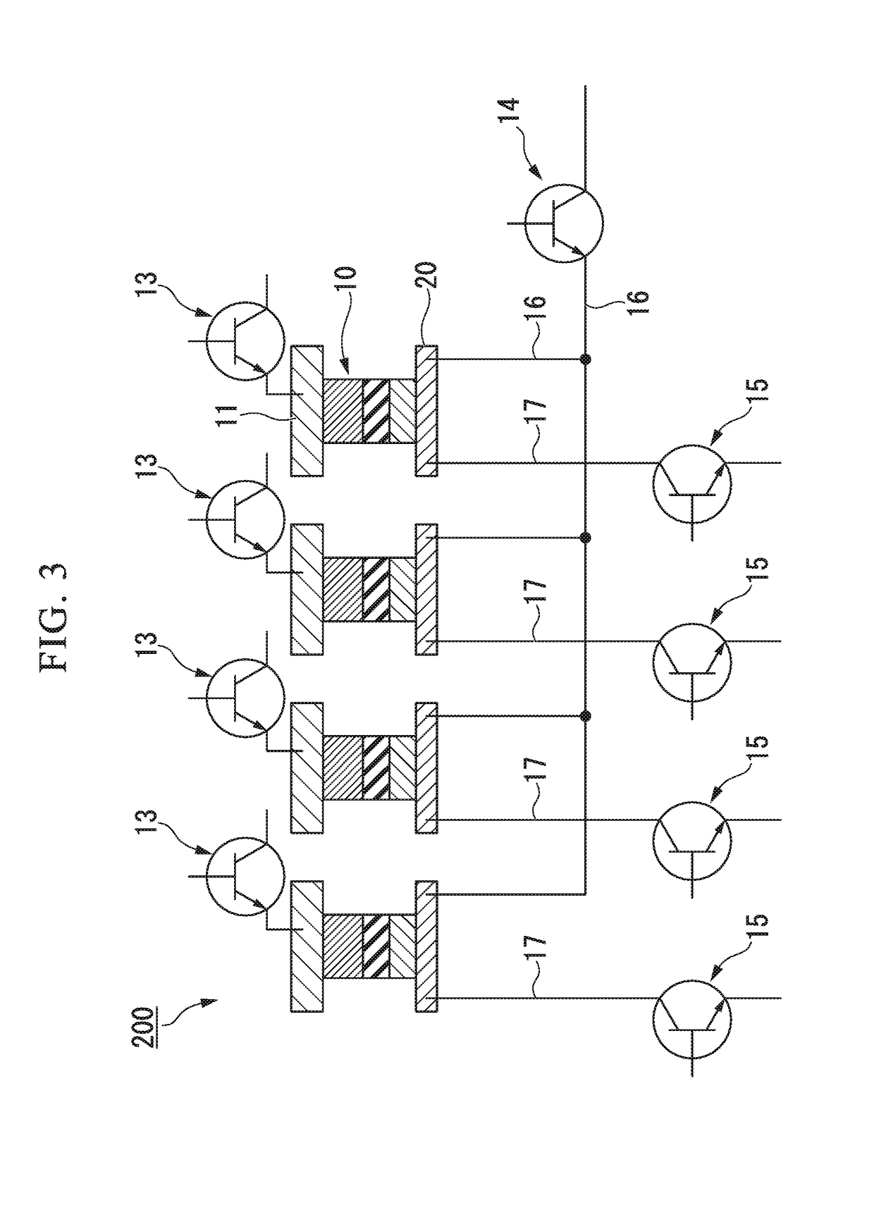
[0040]In the magnetic memory 200 shown in FIG. 1 and the magnetic memory 201 shown in FIG. 2, a first control element 13, a second control element 14, and a first cell selection element 15 are connected to one drive element 100. Known transistors such as a field-effect transistor (FET) are used for such control elements.

[0041]When the first control element 13 and the first cell selection element 15 are operated (are brought into an “ON” sta...

second embodiment

[0127]FIG. 9 is a schematic diagram of a circuit structure of a magnetic memory according to a second embodiment. FIG. 10 is a schematic perspective view of the circuit structure of the magnetic memory according to the second embodiment. In addition, FIG. 11 is a schematic cross-sectional view of a main part in the vicinity of a magnetoresistance effect element of the magnetic memory according to the second embodiment. Components the same as those in the first embodiment will be denoted with the same reference numerals.

[0128]A magnetic memory 204 according to the second embodiment is different from the magnetic memory 200 according to the first embodiment in that a fourth wiring 40 and a second cell selection element 41 are included.

[0129]The fourth wiring 40 connects the magnetoresistance effect elements 10 to the second cell selection elements 41. One end of the magnetoresistance effect element 10 of the fourth wiring 40 is connected to a third connection point 20C. The third conn...

third embodiment

[0138]FIG. 12 is a schematic diagram of a circuit structure of a magnetic memory according to a third embodiment. FIG. 13 is a schematic perspective view of a circuit structure of a magnetic memory according to the third embodiment. In the drawings, components the same as those in the first embodiment will be denoted with the same reference numerals.

[0139]A magnetic memory 205 according to the third embodiment is different from the magnetic memory 200 according to the first embodiment in that a data erasing element 50 and a fifth wiring 51 are included.

[0140]As shown in FIG. 12 and FIG. 13, the data erasing element 50 is connected to the third wirings 17 connected to the spin-orbit torque wirings 20. The data erasing element 50 is connected to the second connection point 20B of the spin-orbit torque wiring 20 through the fifth wiring 51 and the third wirings 17.

[0141]A known switching element can be used as the data erasing element 50. For example, a transistor element represented b...


PUM


Abstract

A magnetic memory includes magnetoresistance effect elements, each of which includes a first ferromagnetic metal layer in which a magnetization direction is fixed, a second ferromagnetic metal layer for a magnetization direction to be changed, and a nonmagnetic layer provided between the first ferromagnetic metal layer and the second ferromagnetic metal layer, a first wiring connected to the first ferromagnetic metal layer of at least one magnetoresistance effect element, spin-orbit torque wirings, each of which is connected to each of the second ferromagnetic metal layers of the magnetoresistance effect elements and extend in a direction intersecting a lamination direction of the magnetoresistance effect element, one first control element connected to the first wiring, one second control element connected to each of first connection points of the spin-orbit torque wirings, and first cell selection elements, each of which is connected to each of second connection points of the spin-orbit torque wirings.

Description

TECHNICAL FIELD[0001]The present invention relates to a magnetic memory.[0002]Priority is claimed on Japanese Patent Application No. 2016-050266, filed Mar. 14, 2016, and Japanese Patent Application No. 2016-182359, filed Sep. 16, 2016, the content of which is incorporated herein by reference.BACKGROUND ART[0003]Giant magnetoresistance (GMR) elements and tunneling magnetoresistance (TMR) elements are known as magnetoresistance effect elements. GMR elements are composed of a multi-layer film including a ferromagnetic layer and a nonmagnetic layer. In TMR elements, an insulating layer (tunnel barrier layer, barrier layer) is used as a nonmagnetic layer. Generally, an element resistance of a TMR element is higher than an element resistance of a GMR element. However, a magnetoresistance (MR) ratio of a TMR element is higher than an MR ratio of a GMR element. Magnetoresistance effect elements are being focused on as magnetic sensors, high frequency components, magnetic heads and nonvolat...

Claims


Application Information

Patent Timeline
IPC IPC(8): H01L43/08H01L43/06H01L43/04H01L43/10G01R33/09H01L27/22G11C11/16G11C11/18
CPCH01L43/08H01L43/06H01L43/04H01L43/10G01R33/098H01L27/228G11C11/161G11C11/1675G11C11/18G01R33/093G01R33/1284H10B61/22H10N50/10H10B99/00H10N50/85H10N52/00H10N52/80
Inventor SASAKI, TOMOYUKI
Owner TDK CORPARATION
Learn More