Conformal mesh for thermal imaging
- Summary
- Abstract
- Description
- Claims
- Application Information
AI Technical Summary
Benefits of technology
Problems solved by technology
Method used
Image
Examples
example 1
Array Methodology for Thermal Sensing
[0054]The thermal sensing mesh consists of an m-by-n matrix of gold thermal resistor network. But instead of having m×n number of individually addressable sensors, only m+n number of sensors are used to address the individual entries of the m-by-n matrix. The significance of this sensor configuration is obvious at large values of m and / or n.
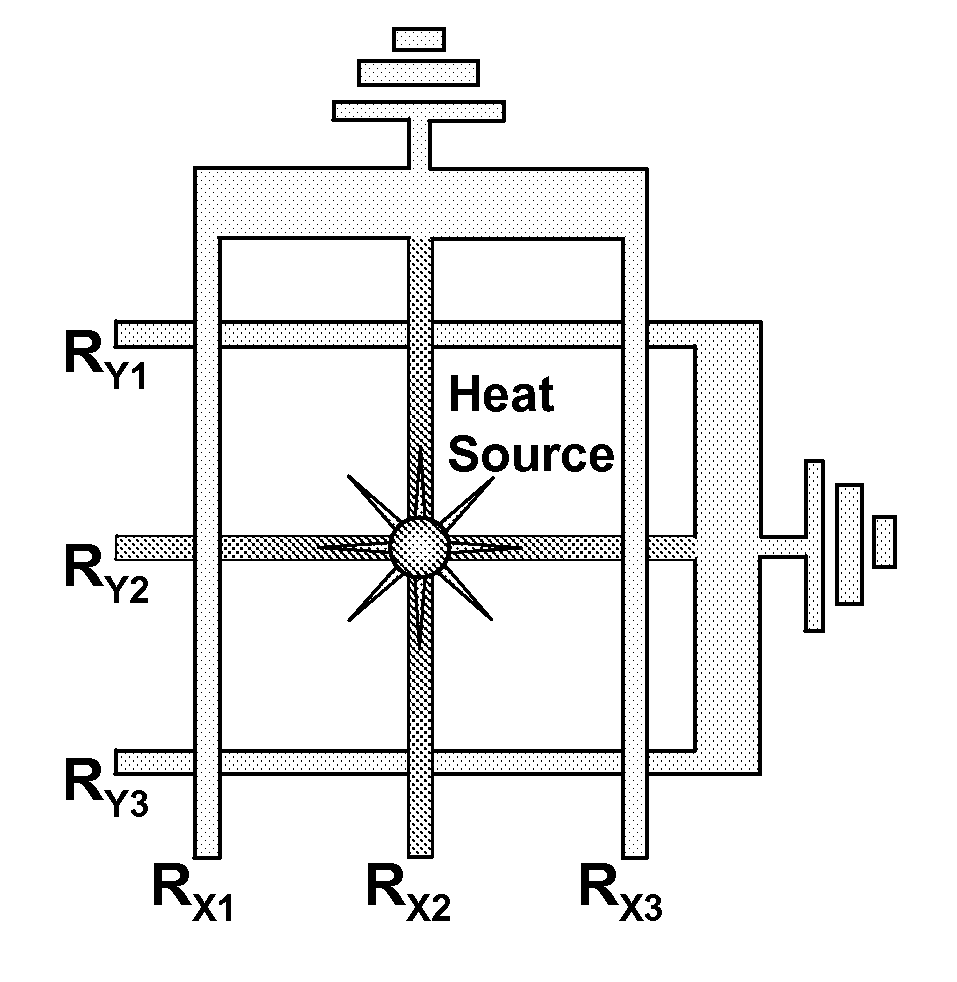
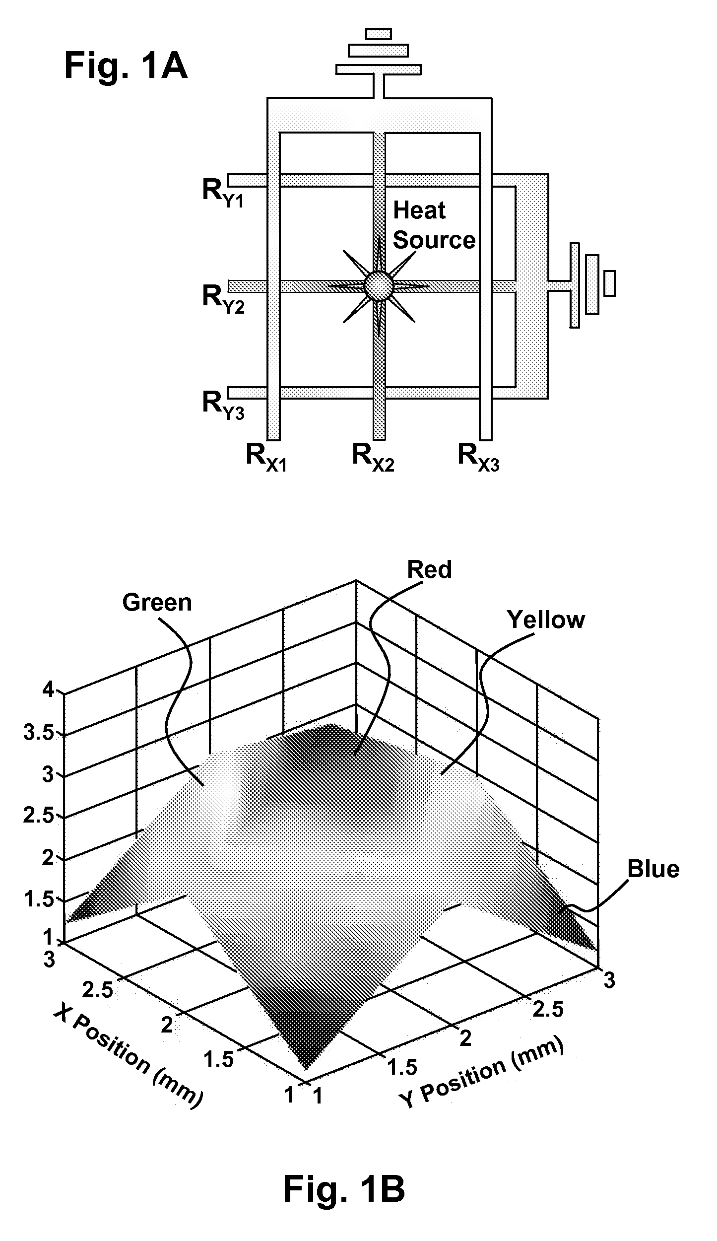
[0055]The sensing of a localized heat source is accomplished by the joint entry of two layers of insulated thermal sensors. The bottom layer consists of m rows of gold thermal resistor named Ry1 to Rym; the top layer consists of n columns of thermal resistor named Rx1 to Rxn (see FIG. 1A for n=m=3). Consider an ideal localized heat source over the point (i, j) on the matrix. As a consequence of the elevated temperature, the corresponding Ryi and Rxj of the thermal resistors increases. The percentage change of resistance is calculated and recorded. The entry Z(i, j) is determined by the product of the percentag...
example 2
Fabrication of Conformable Array
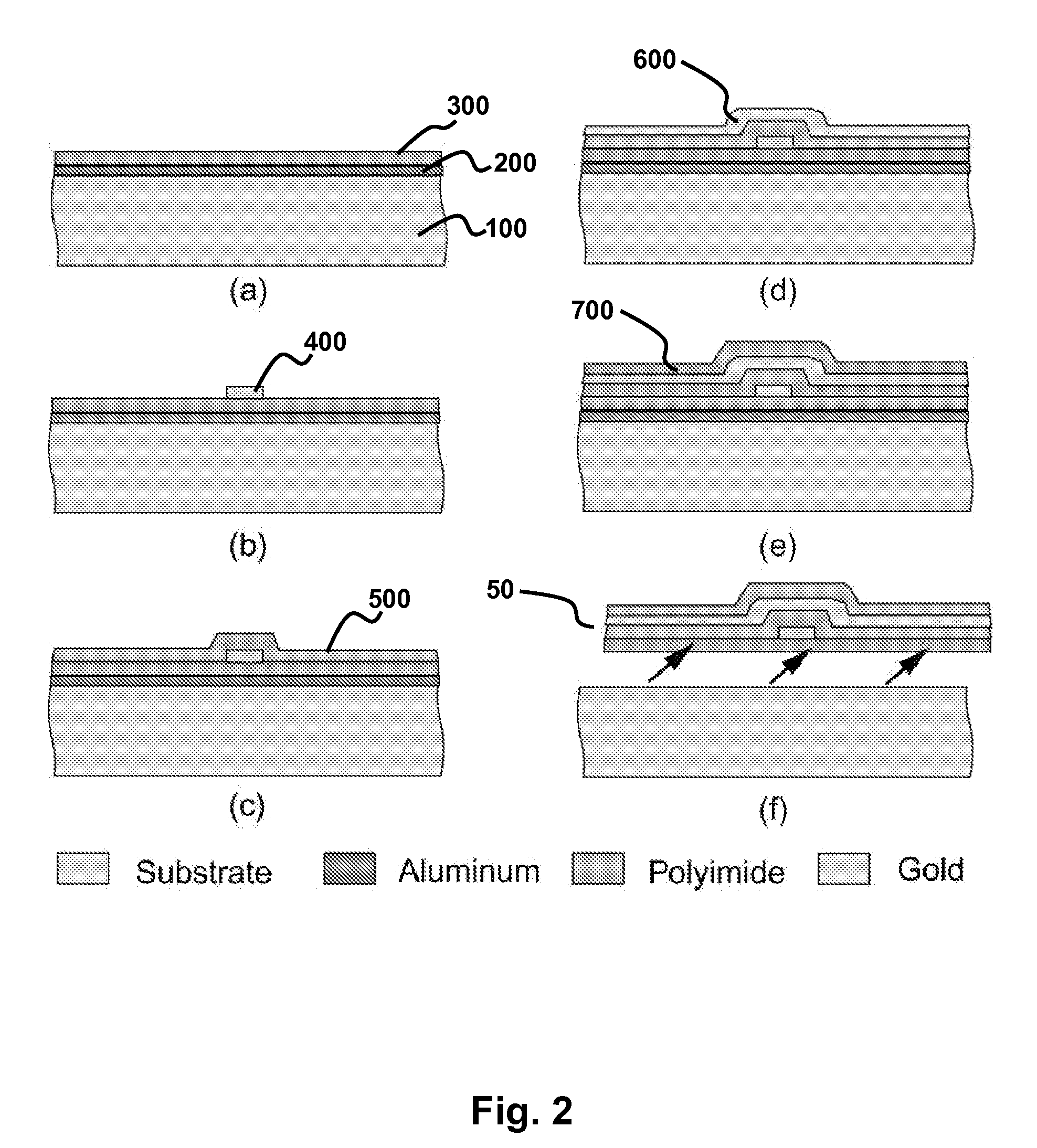
[0059]An example of a fabrication process for making a thermal imaging mesh is summarized in FIG. 2. First, 2000 Å of Al is evaporated onto a 2-inch Si wafer 100 as sacrificial layer 200. On top of the Al layer 200, a first layer of polyimide 300 is spun on, patterned and cured (FIG. 2A). The resultant thickness is about 6 μm. This thick layer of polyimide serves as the base structural layer of the fabric. Then the first layer of 5000 Å gold is evaporated and patterned into 50 μm wide lines 400. These resistor lines form the rows of the thermal resistor network (FIG. 2B). On top of the first gold layer, a second layer of polyimide 500 is spun on, patterned and cured. The resultant thickness is about 1 μm (FIG. 2C). This thin layer of polyimide serves as the insulation layer 500 between the first and second layer of gold thermal resistors. Following the insulation layer, the second layer of 5000 Å gold is evaporated and patterned into 50 μm wide lines ...
example 3
Thermal Imager Testing
[0065]Packaging: A 25×25 matrix thermal imaging mesh is tested. Instead of 625 individual thermal sensors, only 50 thermal sensors are used to address the individual entries of the 25×25 matrix. The number of sensors required and corresponding wiring is greatly reduced.
[0066]The sample is about 5 cm long across the diagonal. To simplify testing, the sample is packaged to a PCB board with wires routed to 25-pin cable connectors (FIG. 7A). A square opening approximately the size of the sample is first milled out from the PCB board. Electrical connections between the mesh and the PCB board are then achieved using methods known in the art such as ACF (anisotropic conductive film). ACF is originally developed for the LCD panel industry and is useful for electrically connecting flexible structures to rigid surfaces. It exhibits excellent conductivity in the vertical direction in contrast to very large resistance in the lateral direction. It is an excellent solution t...
PUM
| Property | Measurement | Unit |
|---|---|---|
| Thickness | aaaaa | aaaaa |
| Thickness | aaaaa | aaaaa |
| Thickness | aaaaa | aaaaa |
Abstract
Description
Claims
Application Information


