Pattern defect detection method

a pattern defect and detection method technology, applied in the field of pattern defect detection methods, can solve the problems of inability to detect defects based on the brightness of patterns, incorrect pattern defect detection, etc., and achieve the effect of higher accuracy

Active Publication Date: 2019-01-24
TASMIT INC
View PDF1 Cites 0 Cited by
  • Summary
  • Abstract
  • Description
  • Claims
  • Application Information

AI Technical Summary

Benefits of technology

[0007]Therefore, according to an embodiment, there is provided a pattern defect detection method capable of detecting a pattern defect of a semiconductor integrated circuit with higher accuracy.
[0013]According to the above-described embodiments, the standard range is determined using the mass data of the brightness index value, and each brightness index value is compared with the standard range. By using such mass data, the defect inspection of the semiconductor integrated circuit with the voltage contrast can be performed with higher accuracy.

Problems solved by technology

However, in the interconnect defect inspection using the voltage contrast, the reliability of inspection depends on a method of generating the image of the non-defective product to be used and the image of the inspection target pattern.
However, in the above-described method using design data for creating an image of a non-defective product, the pattern defect detection is not correctly performed if there is a variation in the brightness of non-defective products.
Further, since the positions of the pattern edges are compared in the die-to-database comparison, it is impossible to detect a defect based on the brightness of the pattern.

Method used


Image

  • Pattern defect detection method
  • Pattern defect detection method
  • Pattern defect detection method

Examples


Embodiment Construction

[0023]Hereinafter, embodiments will be described in detail with reference to the drawings.

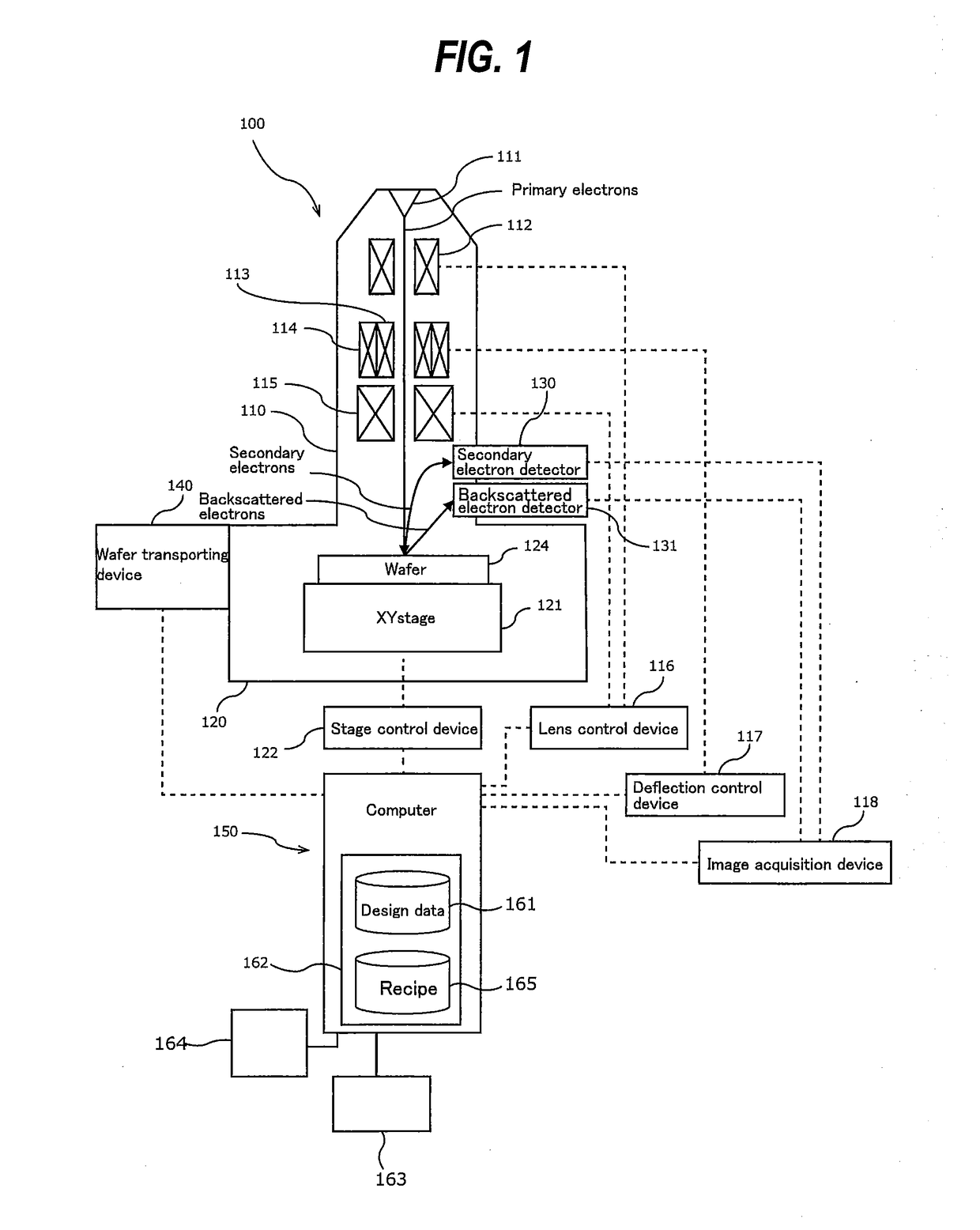
[0024]FIG. 1 is a schematic diagram showing an embodiment of a pattern defect detection apparatus including a scanning electron microscope. As shown in FIG. 1, the pattern defect detection apparatus includes a scanning electron microscope 100 and a computer 150 for controlling operations of the scanning electron microscope. The scanning electron microscope 100 includes an electron gun 111 that emits an electron beam composed of primary electrons (charged particles), a converging lens 112 that converges the electron beam emitted from the electron gun 111, an X deflector 113 that deflects the electron beam in an X direction, a Y deflector 114 for deflecting the electron beam in a Y direction, and an objective lens 115 for focusing the electron beam on a wafer 124 which is a specimen.

[0025]The converging lens 112 and the objective lens 115 are coupled to a lens control device 116, and operations o...


PUM

PropertyMeasurementUnit
pattern defect detectionaaaaaaaaaa
scanning electron microscopeaaaaaaaaaa
shapeaaaaaaaaaa

Abstract

A pattern defect detection method capable of detecting a pattern defect of a semiconductor integrated circuit with higher accuracy is disclosed. The pattern defect detection method includes: extracting an image of an inspection target pattern from an image of a specimen; identifying a reference pattern from design data, the reference pattern having the same shape and the same position as those of the inspection target pattern; calculating a brightness index value indicating a brightness of an entirety of the inspection target pattern; repeating said extracting an inspection target pattern, said identifying a reference pattern, and said calculating a brightness index value, thereby building mass data containing brightness index values of inspection target patterns and corresponding reference patterns; determining a standard range of brightness index value based on the brightness index values contained in the mass data; and detecting a defect of the inspection target pattern based on whether or not the calculated brightness index value is within the standard range.

Description

CROSS REFERENCE TO RELATED APPLICATION[0001]This document claims priority to Japanese Patent Application No. 2017-123092 filed Jun. 23, 2017, the entire contents of which are hereby incorporated by reference.BACKGROUND[0002]One example of a method of inspecting a defect of interconnects in a semiconductor integrated circuit is an inspection method using a voltage contrast using a scanning electron microscope. This technique utilizes the fact that a brightness of a pattern on an SEM image decreases when there is an open defect or a short defect in an interconnect underlying the pattern. In this method, an SEM image of a non-defective product and an SEM image of the inspection target pattern are compared with each other to thereby detect an interconnect defect.[0003]FIG. 9 is a schematic view showing an SEM image including a non-defective contact hole and a defective contact hole. As shown in FIG. 9, a brightness of a defective contact hole 601 is lower than that of a non-defective co...

Claims


Application Information

Patent Timeline
Patent Type & Authority Applications(United States)
IPC IPC(8): G01R31/307G01N21/956G06T7/00G01N21/95
CPCG01R31/307G01N21/95607G06T7/001G01N21/9505G06T2207/30148G01N2021/95615G03F7/70625
Inventor SHIMODA, RYO
Owner TASMIT INC
Why Eureka
Try Eureka