
Method of forming pattern of cured product as well as production methods for processed substrate, optical component, circuit board, electronic component, imprint mold and imprint pretreatment coating material

a technology of cured products and patterns, applied in the field of forming patterns of cured products, can solve the problems of long filling and low throughput, and achieve the effect of improving the yield (throughput) of the sst-nil process and significantly reducing the yield

Active Publication Date: 2019-01-31
CANON KK
View PDF0 Cites 7 Cited by
  • Summary
  • Abstract
  • Description
  • Claims
  • Application Information

AI Technical Summary

Benefits of technology

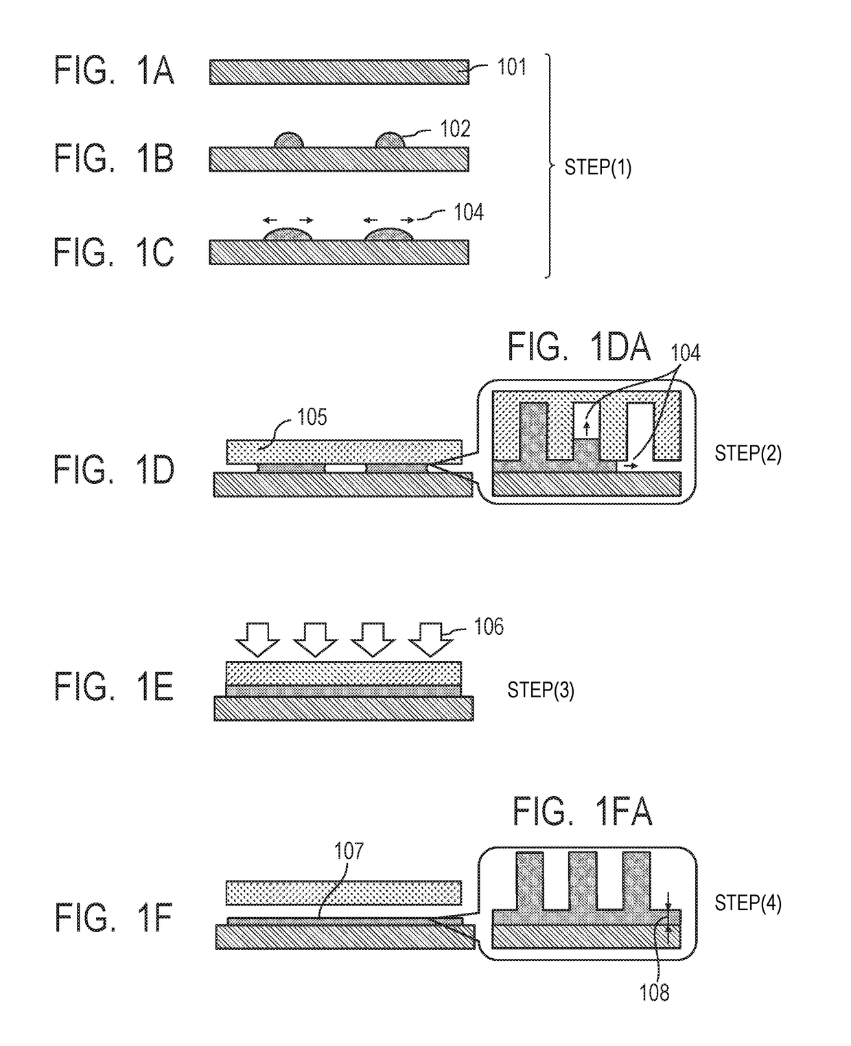
The present invention aims to improve the yield (throughput) of the SST-NIL process. This is particularly useful when the pattern transfer on the substrate and the curing of the mixture layer obtained by mixing curable compositions is repeated with one mold multiple times. This can lead to breakage or clogging of the groove / land pattern of the mold which causes issues in subsequent transfer patterns and reduces yield. The present invention provides a solution to this problem and improves the yield (throughput) of the imprint process.

Problems solved by technology

The photo-nanoimprint technology disclosed in Japanese Patent Application Laid-Open No. 2010-073811 has involved a problem in that a time period (filling time) from the initiation of the contact of the mold to the completion of the spread and the fill is long, and hence throughput is low.

Method used


Image

  • Method of forming pattern of cured product as well as production methods for processed substrate, optical component, circuit board, electronic component, imprint mold and imprint pretreatment coating material
  • Method of forming pattern of cured product as well as production methods for processed substrate, optical component, circuit board, electronic component, imprint mold and imprint pretreatment coating material
  • Method of forming pattern of cured product as well as production methods for processed substrate, optical component, circuit board, electronic component, imprint mold and imprint pretreatment coating material

Examples


example 1

[0253](1) Preparation of Curable Composition (α1-1)

[0254]A component (A), a component (B), a component (C), and a component (D) described below were blended, and the blend was subjected to circulation filtration with an ion filter, a 10-nanometer nylon filter, and a 5-nanometer HDPE filter. The circulation filtration was performed for a time period corresponding to about 8 passes (the time period is equal to a liquid delivering period that eight times volume of the filtrate is processed) to prepare a curable composition (α1-1) of Example 1.

(1-1) Component (A):100parts by weight in total 1,12-Dodecanediol diacrylate100parts by weight(manufactured by Wanda Science):(1-2) Component (B):0parts by weight in totalThe component (B) was not added.(1-3) Component (C):0parts by weight in totalThe component (C) was not added.(1-4) Component (D):33,000parts by weight in totalPropylene glycol monomethyl33,000parts by weightether acetate (manufactured byTokyo Chemical Industry Co.,Ltd., abbreviat...

example 2

[0258](1) Preparation of Curable Composition (α1-2)

[0259]A curable composition (α1-2) was prepared in the same manner as in Example 1 except that the component (A) was changed to 30 parts by weight of 1,12-dodecanediol diacrylate (manufactured by Wanda Science) and 70 parts by weight of dimethyloltricyclodecane diacrylate (manufactured by Sartomer, trade name: SR833s).

[0260](2) Measurement of Number Concentration of Particles in Curable Composition (α1-2)

[0261]The number concentration of particles was measured in the same manner as in Example 1. The number concentration (average) of particles each having a particle diameter of 0.07 μm or more in the curable composition (α1-2) was 36.5 particles / mL.

example 3

[0262](1) Preparation of Curable Composition (α2-1)

[0263]A component (A), a component (B), a component (C), and a component (D) described below were blended, and the blend was subjected to circulation filtration with an ion filter, a 10-nanometer nylon filter, and a 5-nanometer HDPE filter. The circulation filtration was performed for a time period corresponding to about 8 passes to prepare a curable composition (α2-1) of Example 3.

(1-1) Component (A):94parts by weight in total Isobornyl acrylate9.0parts by weight(manufactured by Kyoeisha ChemicalCo., Ltd., trade name: IB-XA): Benzyl acrylate (manufactured38.0parts by weightby Osaka Organic Chemical IndustryLtd., trade name: V#160): Neopentyl glycol diacrylate47.0parts by weight(manufactured by Kyoeisha ChemicalCo., Ltd., trade name: NP-A):(1-2) Component (B):3parts by weight in total Lucirin TPO3parts by weight(manufactured by BASF):(1-3) Component (C):2.1parts by weight in total SR-730 (manufactured by1.6parts by weightAoki Oil In...


PUM

PropertyMeasurementUnit
particle diameteraaaaaaaaaa
widthaaaaaaaaaa
widthaaaaaaaaaa

Abstract

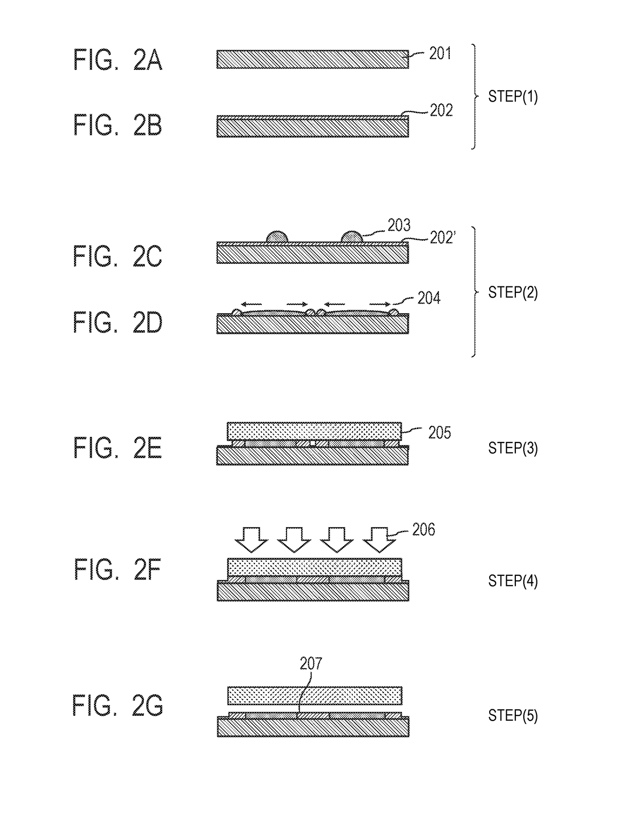
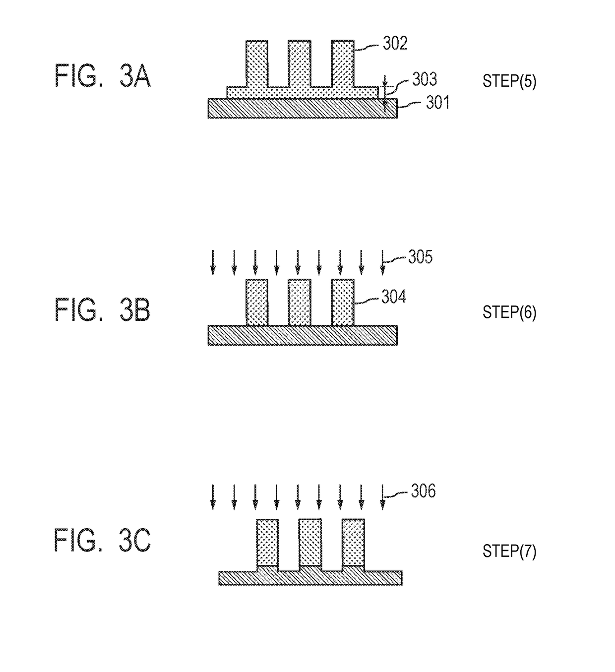
Provided is a method of producing a cured product pattern, including: a first step (arranging step) of arranging a layer formed of a curable composition (α1′) that is the components of the curable composition (α1) except the component (D) serving as a solvent on a substrate; and a second step (applying step) of applying droplets of a curable composition (α2) discretely onto the layer formed of the curable composition (α1), the curable composition (α1) having a number concentration of particles each having a particle diameter of 0.07 μm or more of less than 2,021 particles / mL, and the curable composition (α1′) having a surface tension larger than that of the curable composition (α2).

Description

CROSS-REFERENCE TO RELATED APPLICATIONS[0001]This application is a Continuation of International Patent Application No. PCT / JP2017 / 013501, filed Mar. 31, 2017, which claims the benefit of U.S. Provisional Patent Application No. 62 / 319,878, filed Apr. 8, 2016, both of which are hereby incorporated by reference herein in their entirety.BACKGROUND OF THE INVENTIONField of the Invention[0002]The present invention relates to a method of forming a cured product pattern, a method of producing a processed substrate, a method of producing an optical component, a method of producing a circuit board, a method of producing an electronic component, a method of producing an imprint mold, and a material for an imprint pretreatment coating.Description of the Related Art[0003]There has been a growing requirement for miniaturization in a semiconductor device, a MEMS, or the like, and a photo-nanoimprint technology has particularly been attracting attention.[0004]In the photo-nanoimprint technology, a...

Claims


Application Information

Patent Timeline
Patent Type & Authority Applications(United States)
IPC IPC(8): B29C59/16B29C59/00H01L21/027H01L21/02
CPCB29C59/16B29C59/007B29C59/002H01L21/0273H01L21/022B82Y10/00B82Y40/00B29C2791/005B29K2033/12G03F7/0002G03F7/027G03F7/004G03F7/028G03F7/168H01L21/0274G03F7/161
Inventor KATO, JUNHONMA, TAKESHIITO, TOSHIKITSUZUKI, HIDETOSHI
Owner CANON KK
Learn More