Optical modulator and optical transmission device using optical modulator

Active Publication Date: 2019-02-14
SUMITOMO OSAKA CEMENT CO LTD
View PDF4 Cites 0 Cited by
  • Summary
  • Abstract
  • Description
  • Claims
  • Application Information

AI Technical Summary

Benefits of technology

[0046]From the above-described background, in an optical modulator including, on the same substrate, a bias electrode to which a bias voltage and a dither signal are applied, and a photo detector that monitors intensity of a dither si

Problems solved by technology

However, as described above, in an optical modulator (for example, DP-QPSK modulator) that uses a plurality of bias electrodes, a new problem for a bias voltage control, which does not occur in an optical modulator including one bias electrode, may occur.
This problem is specific to the optical modulator that uses the plurality of bias electrodes, and the following phenomenon is observed.When a dither signal is applied to one bias electrode, an optical characteristic control (phase adjustment or temperature drift compensation) in one or a plurality of other bias electrodes may become unstable.
As a result, they obtained a finding that the cause of the unstable phenomenon is a surface acoustic wave (SAW) that occurs when a dither signal is applied to the bias electrodes on an LN substrate.
According to this, the other bias electrode receives the dither signal that is applied to the one bias electrode, and the dither signal that is received give interference to a bias control operation in the other bias electrode and has an adverse effect on the bias control operation.
Therefore, the unstable phenomenon occurs between bias electrodes which are not adjacent or close to each other, and the unstable phenomenon occurs depending on the environme

Method used


Image

  • Optical modulator and optical transmission device using optical modulator
  • Optical modulator and optical transmission device using optical modulator
  • Optical modulator and optical transmission device using optical modulator

Examples


Example

First Embodiment

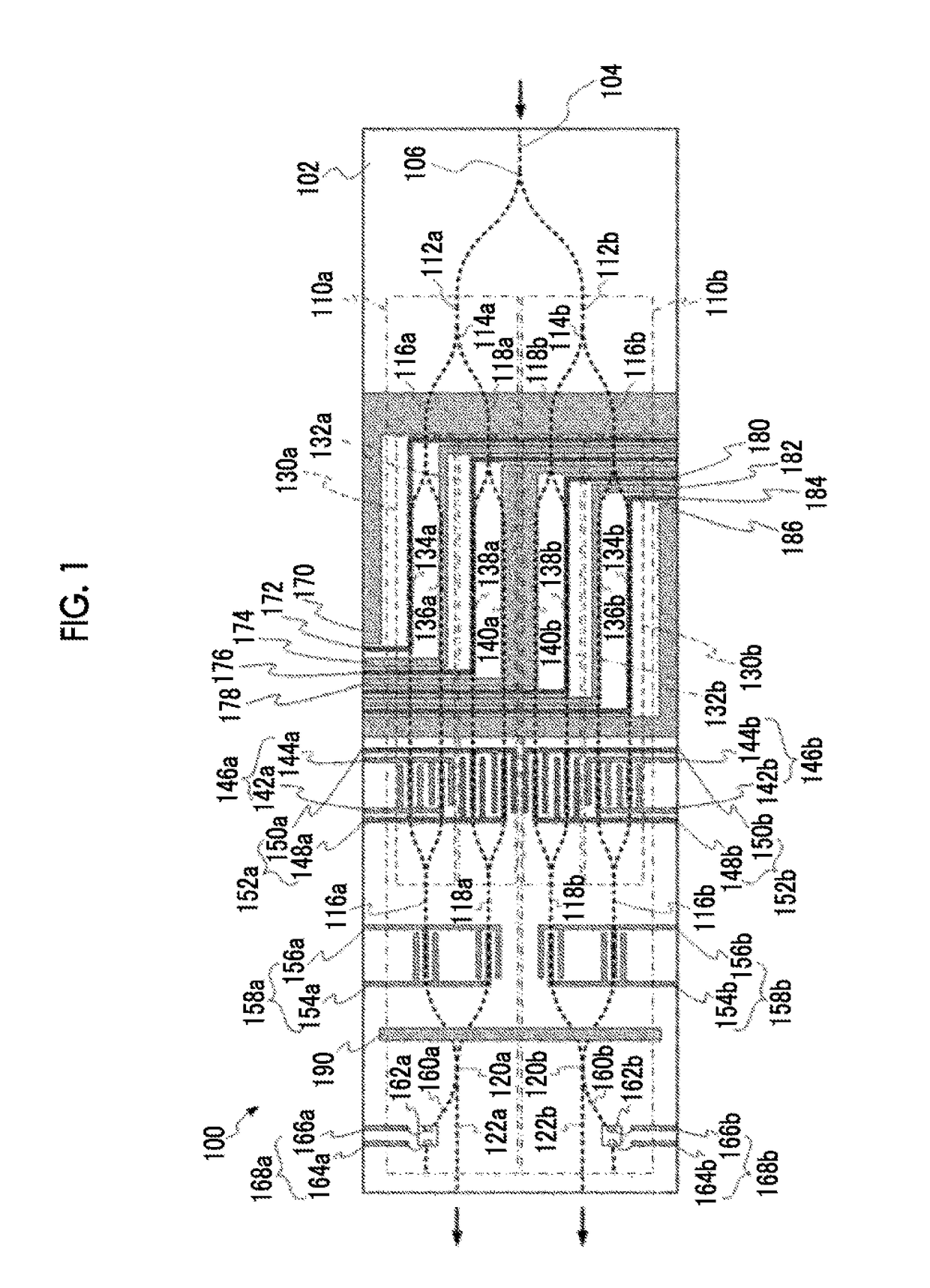
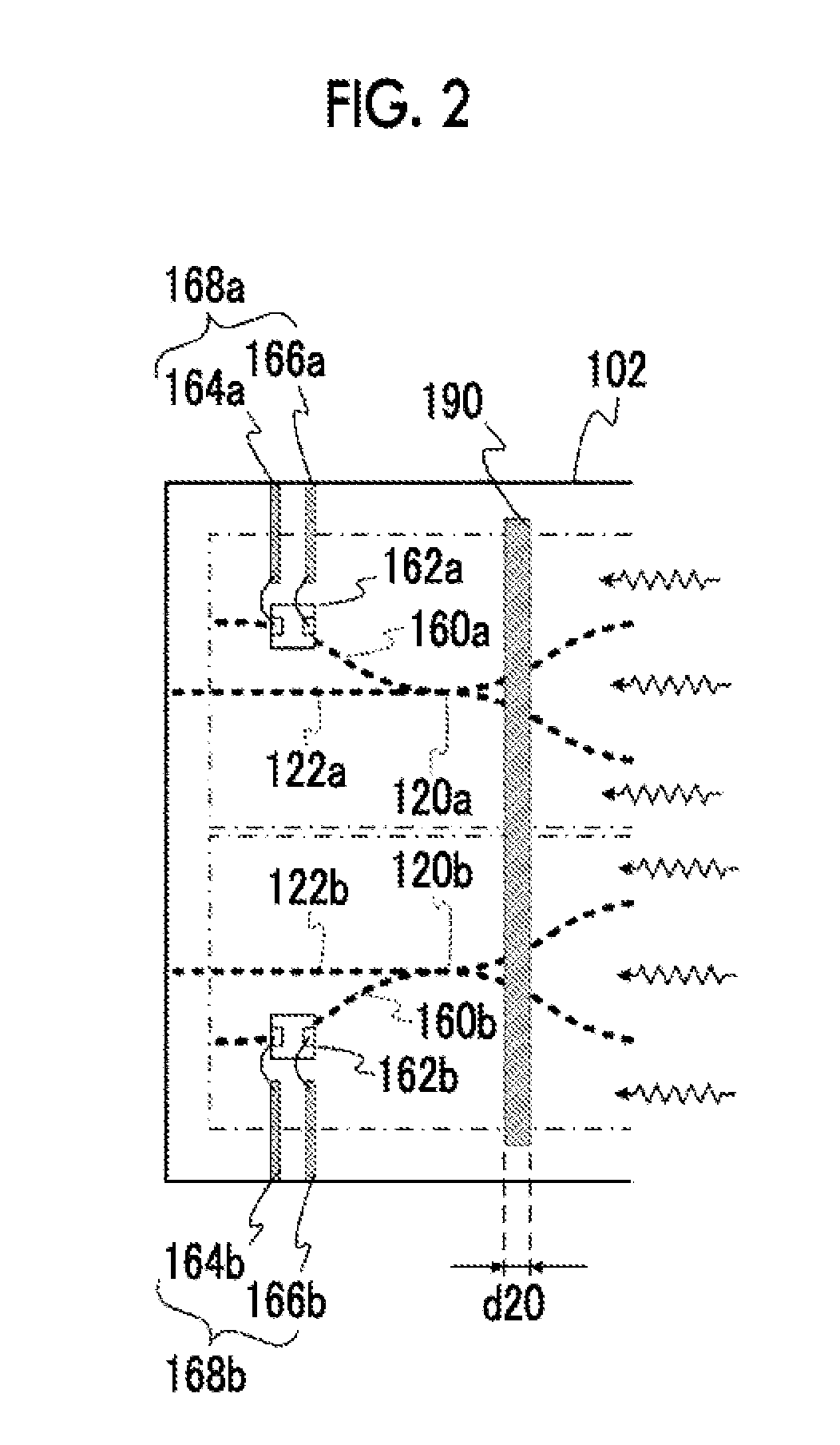
[0074]First, description will be given of a first embodiment of the invention. FIG. 1 is a view illustrating a configuration of an optical modulator according to the first embodiment of the invention. As described above, an optical modulator 100 according to this embodiment is, for example, the DP-QPSK modulator, and a basic configuration is the same as in the DP-QPSK modulator 1300 of the related art as illustrated in FIG. 13. That is, for example, the optical modulator 100 is constituted by a nest-type Mach-Zehnder optical waveguide (a bold dotted line in the drawing) that is formed on the LN substrate 102, and an electrode (a hatched portion in the drawing). In the optical modulator, light beams from light source (not illustrated) such as a laser diode are incident from a right direction in the drawing, and modulated light beams are emitted from a left direction in the drawing. For example, the emitted light beams are multiplexed by a space optical system, and are...

Example

First Modification Example

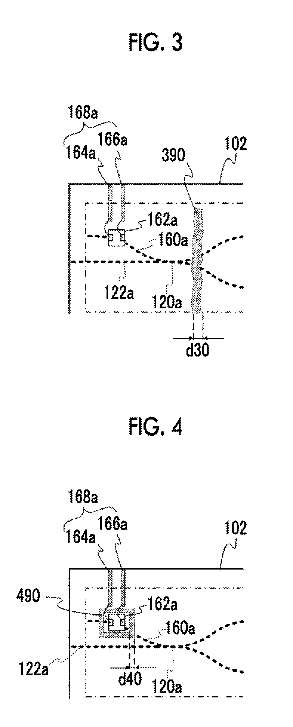
[0089]First, description will be given of a first modification example of the surface acoustic wave suppressing unit that is used in the optical modulator 100 illustrated in FIG. 1. In this modification example, as the surface acoustic wave suppressing unit, a resin, which absorbs the surface acoustic wave, is used instead of the guard pattern 190.

[0090]FIG. 3 is a view illustrating a surface acoustic wave suppressing unit, which can be used instead of the guard pattern 190, according to this modification example. Furthermore, in FIG. 3, the same constituent element as the constituent element illustrated in FIG. 1 and FIG. 2 will be indicated by the same reference numeral as in FIG. 1 and FIG. 2, and description in FIG. 1 and FIG. 2 will be cited.

[0091]In the modification example illustrated in FIG. 3, as the surface acoustic wave suppressing unit, a resin 390 is applied on the LN substrate 102 between a region in which the bias electrodes 146a, 152a, 146b,...

Example

Second Modification Example

[0093]Next, description will be given of a second modification example of the surface acoustic wave suppressing unit that is used in the optical modulator 100 illustrated in FIG. 1.

[0094]FIG. 4 is a view illustrating a surface acoustic wave suppressing unit, which can be used instead of the guard pattern 190, according to this modification example. Furthermore, in FIG. 4, the same constituent element as the constituent element illustrated in FIG. 1 and FIG. 2 will be indicated by the same reference numeral as in FIG. 1 and FIG. 2, and description in FIG. 1 and FIG. 2 will be cited.

[0095]In this modification example, as illustrated in FIG. 4, as the surface acoustic wave suppressing unit, a rectangular guard pattern 490, which is formed from a metal (for example, gold (Au)) that absorbs the surface acoustic wave, is formed on the LN substrate 102 to surround the mounting portion (or mounting region) of the photo detector 162a against the region in which the...


PUM


Abstract

To perform a stable bias control by improving detection accuracy of intensity of an dither signal component, which is detected by a photo detector, in an optical modulator including a bias electrode to which a dither signal is applied, and a photo detector that monitors an optical signal propagating through the inside of an optical waveguide in the same substrate. The optical modulator includes: a substrate having a piezoelectric effect (102); an optical waveguide (116a or the like) that is formed on the substrate; a bias electrode (158a or the like) that controls an optical wave that propagates through the optical waveguide; and a photo detector (168a or the like) that is formed on the substrate, and monitors an optical signal that propagates along the optical waveguide. At least one suppressing unit (190 or the like), which suppresses a surface acoustic wave that propagates from the bias electrode to the photo detector, is disposed between a region in which the bias electrode is formed and a portion in which the photo detector is disposed on the substrate.

Description

TECHNICAL FIELD[0001]Certain embodiments of the present invention relate to an optical modulator and an optical transmission device using the optical modulator, and particularly to, an optical modulator in which a bias electrode and a photo detector that monitors emitted light beams are formed on the same substrate, and an optical transmission device using the optical modulator.BACKGROUND ART[0002]In a high-frequency and large-capacity optical fiber communication system, optical transmission devices to which a waveguide type optical modulator is introduced have been widely used. Among these, an optical modulator, in which LiNbO3 (hereinafter, also referred to as “LN”) having an electro-optic effect is used in a substrate, has been widely used in the high-frequency and large-capacity optical fiber communication system when considering that it is possible to realize optical modulation characteristics in which an optical loss is smaller and a band is wider in comparison to a modulator ...

Claims


Application Information

Patent Timeline
IPC IPC(8): G02F1/01G02F1/225
CPCG02F1/0123G02F1/225G02F2201/58G02F2001/212G02F2201/12G02F2202/20G02F1/212
Inventor MIYAZAKI, NORIKAZUSUGAMATA, TORU
Owner SUMITOMO OSAKA CEMENT CO LTD
Why Eureka
Try Eureka